

Introduction
Hi! 😃 This article will focus on learning to implement the I2C protocol on the STM32F407 Discovery Board and interfacing various devices using it. Here, we will be looking at connecting a Liquid Crystal Display with our MCU. The LCD has an I2C module attached to its back. The Burst Write Sequence in the I2C protocol, is used to send the data and commands to the LCD. I will also be using a Logic Analyzer to capture the SCL and SDA signals.
Working Principle
- I2C Protocol
I2C stands for Inter-Integrated Circuit, it is a multi-master, multi-slave type of protocol. Each master accesses a slave device by its unique I2C address. It supports two values for the communication speed where 100 KHz is the standard speed and 400 KHz is the speed in the Fast Mode. The I2C protocol is referred to as a Synchronous protocol because the master sends the data (SDA) that needs to be transmitted along with the clock (SCL). The slave devices work based on this clock and hence all the operations on the bus are synchronized.
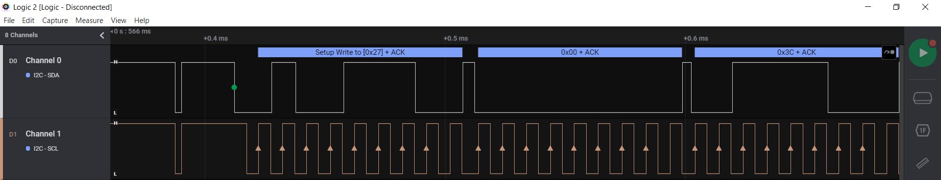
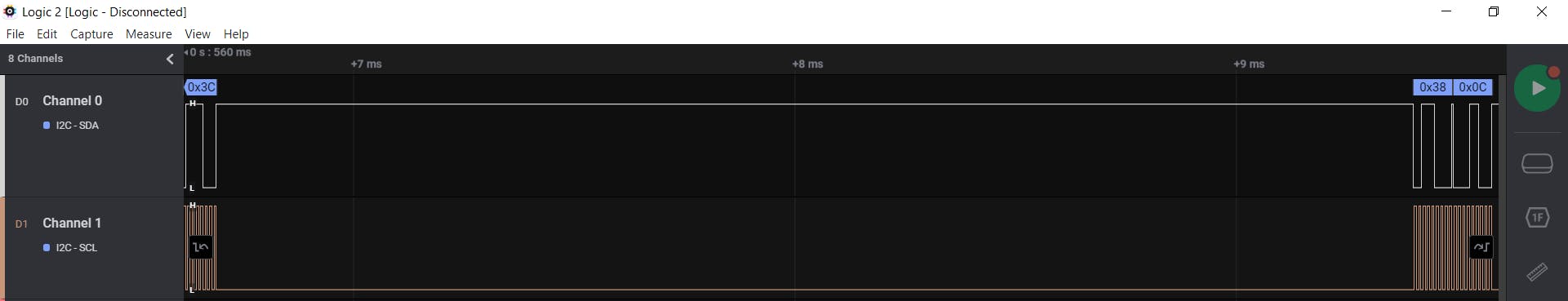
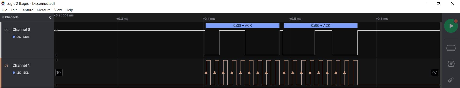
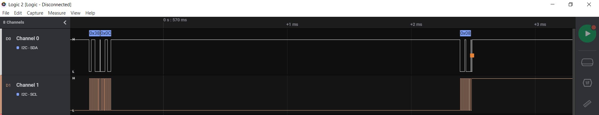
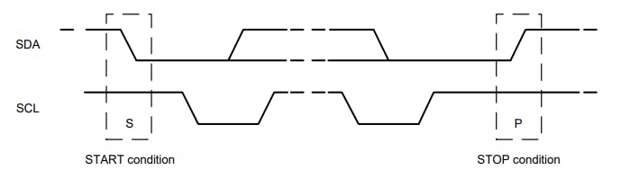
The transmission starts when a START condition is generated by the Master. This condition occurs when SDA goes from a HIGH to a LOW state when SCL is HIGH. Similarly, a STOP condition ends the transmission, when SDA goes from a LOW to a HIGH state when SCL is HIGH. This can be seen below.
A standard I2C transmission looks like the following,
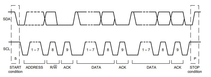
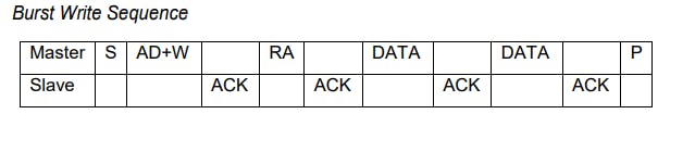
As you can see in the figures above after the START condition is generated the Master sends the address of the device it wants to communicate with, and then tells the device whether it wants to Read from the device or Write to it which is decided by the R/W bit in the frame. Now, according to the STM32 convention the R/W bit is considered to be a part of the Address Field in the I2C frame, whereas in an Arduino suppose, the R/W bit is not the part of the Address Field. So, let's say you have the address of an I2C device that is interfaced with an Arduino. To use the device with an STM32 MCU the address that is used to interface the device with the Arduino needs to be Left-Shifted by 1 and the LSB of the Address Field should be your R/W bit. We will look at this again in a later part of this blog.
After the Address Field, the device that is being communicated with needs to acknowledge the request and send a ACK bit, which is at a LOW state. In a write cycle, once the acknowledgment from the slave device has been received the Master then proceeds to send the Address or Location at which the write operation needs to be performed on the slave device. This request then needs a similar acknowledgment from the slave device as described before. Next, the Master can put the data on the bus that needs to be transmitted and the slave responds with an acknowledgment. This data transmission can continue until the STOP condition is generated by the Master. But the read or write operation can be done only at a specific location or address on the slave device sent by the master in one transmission cycle. To read or write to another register or address on the slave, another transmission cycle needs to be performed. This constitutes the Burst Write Sequence of the I2C Protocol* that we will be utilizing in this blog to interface the LCD.
- LCD and the I2C Module PCF8574T
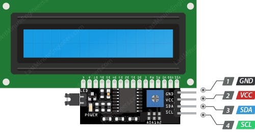
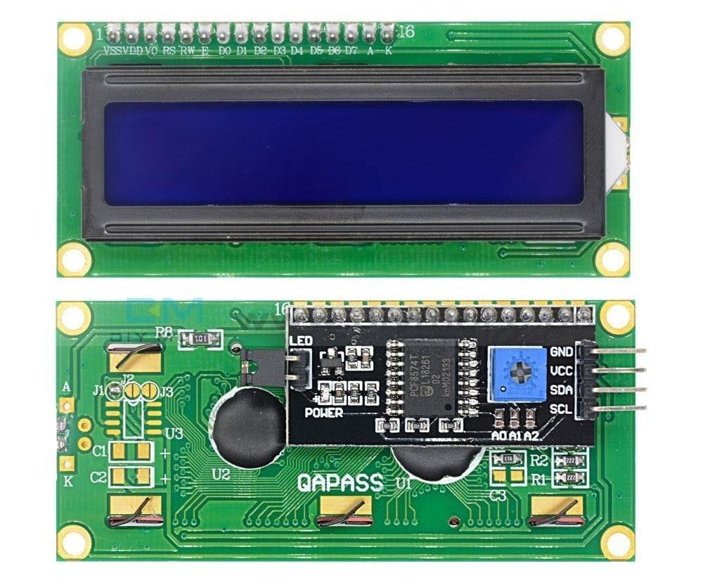
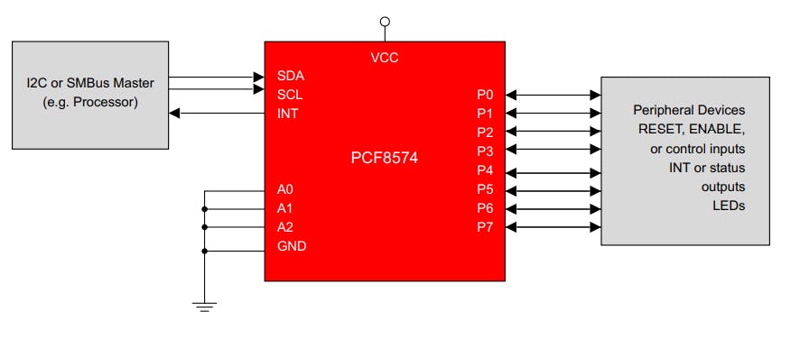
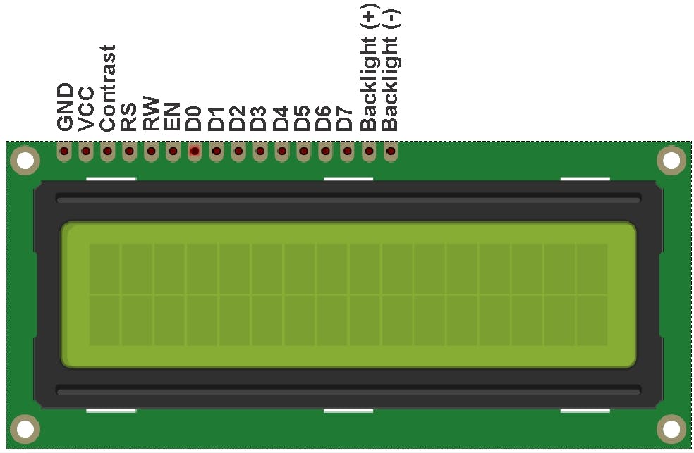
As seen from the figures above there are 8 output pins from P0 - P7 on the PCF8574T module, and they are connected to the LCD pins as follows:
| PCF8574T | 16x2 LCD |
| P0 | RS |
| P1 | R/W |
| P2 | EN |
| P3 | Back Light |
| P4 | D4 |
| P5 | D5 |
| P6 | D6 |
| P7 | D7 |
From the above table, we can infer that since only 4 data pins of the LCD are connected to the I2C module, we will need to use the 4-bit mode of the LCD to interface it. There are 4 input pins which are VCC, SCL, SDA, and GND.
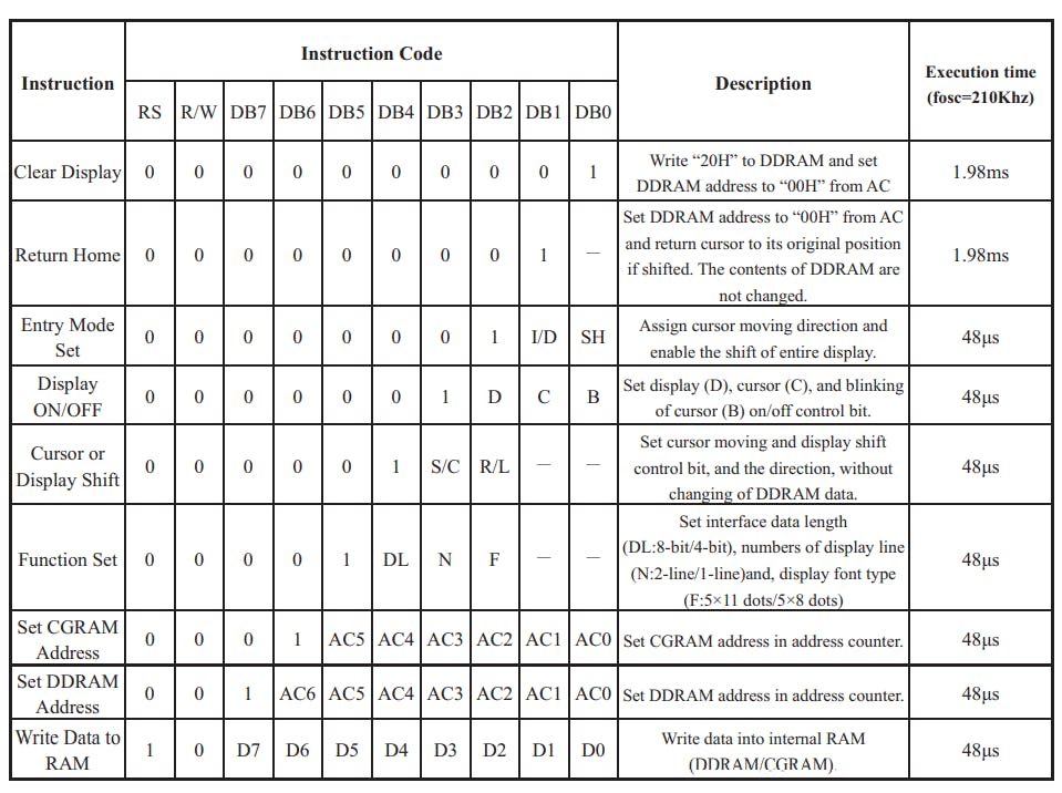
The LCD has 2 registers, namely the Instruction Register and the Data Register. These can be selected using the RS bit which stands for Register Select. When RS bit is set to 0 the Instruction Register is selected, and when it's set to 1 the Data Register is selected. Various commands are needed to initialize the LCD. These should be directed towards the Instruction Register, for configuring the LCD.
The table below shows the various instructions that are needed to initialize the LCD and their corresponding execution time.

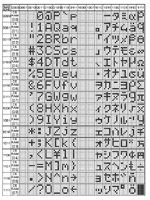
Any character that needs to be displayed on the LCD, can be generated by writing its corresponding code from the Character Generator ROM Pattern. This can be seen below,
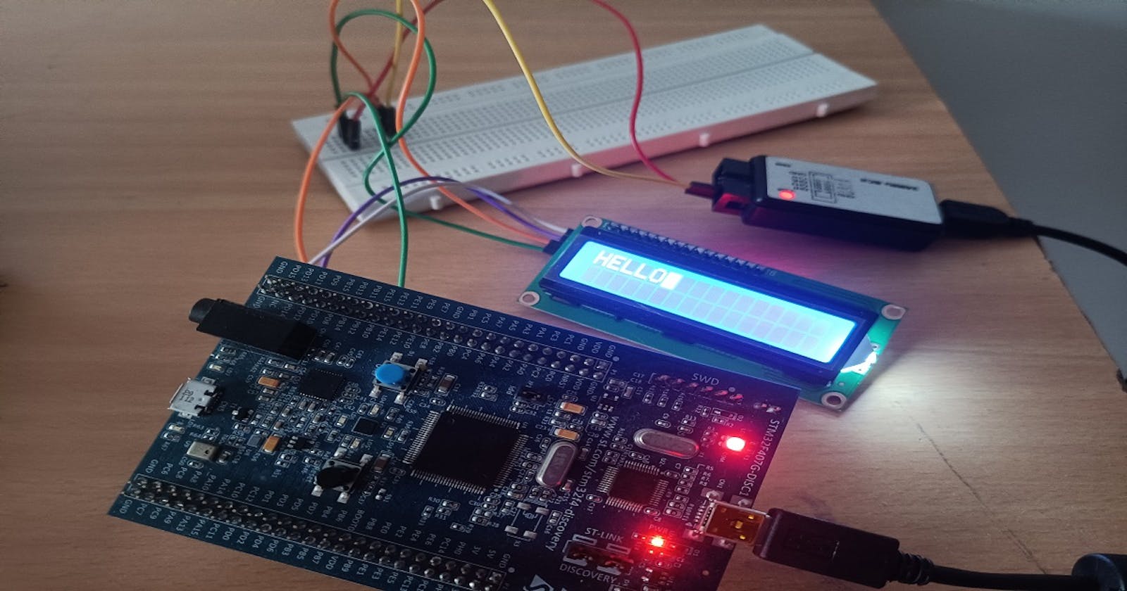
Finally, the connections that need to be made between the LCD and the STM32F407 Discovery Kit can be found in my Github repository which can be accessed by clicking here.
Components Required
An STM32F4 based MCU
A 16x2 LCD with an I2C module attached
A Logic Analyzer (Optional)
A few Jumper wires
A Breadboard (Optional)
And, there you go! 😄. We are all set to begin writing the code for our microcontroller. So, let's get into it.
Programming the MCU
1. Including the necessary Header Files and some comments about the code
/******************************************************************************
* This is the code for interfacing a 16x2 LCD with a I2C module using the
* I2C protocol, and printing "HELLO" on the LCD Screen.
*
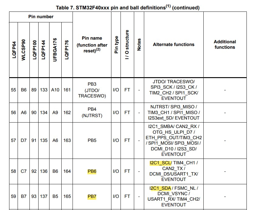
* Configurations are as follows:
* PB6 - I2C1_SCL
* PB7 - I2C1_SDA
* (See Page 58 of the 203 Page user stm32f407vg user manual)
*
* For the I2C Module (PC58574T) to LCD the connections are as follows:
* P0 - RS
* P1 - R/W
* P2 - E
* P3 - Back Light
* P4 - D4
* P5 - D5
* P6 - D6
* P7 - D7
* So, the data byte that we send through the I2C module will be mapped to the
* LCD based on the above configuration. This will be helpful for understanding
* how the data and commands are sent to the LCD in the LCD_Write_Data and
* LCD_Write_Cmd function.
*****************************************************************************/
//Header Files
#include <stm32f4xx.h>
#define ARM_MATH_CM44
These are the header files included at the top of our main.c file. The stm32f4xx.h is the one for our microcontroller and the ARM_MATH_CM4 is for any math operations that we perform in our code.
2. Defining the Slave Device Address and its Register Definitions
//Register Definitions for 1602A I2C LCD
#define LCD_ADDR (0x4E)
#define INST_REG (0x00)
#define DATA_REG (0x40)
Here, as discussed earlier, for converting the I2C Address for LCD into the STM32 convention, we left shift it by 1. So, the device address which was given to be 0x27 is left-shifted by 1. By doing 0x27<<1 we get 0x4E. Hence, the LCD_ADDR is assigned the value of 0x4E. The Instruction Register on the LCD is located at 0x00 and the Data Register is located at 0x40. These values are given to the corresponding macros in the code.
3. Declaring User-Defined Variables
// Variable for clearing ADDR bit
uint8_t clc;
Here, we initialize a variable named clc which will be used in the later part of the code, and we will discuss it then.
4. Declaring User-Defined Functions
//User-defined Function Declarations
void GPIO_Init(void);
void I2C_Init(void);
void I2C_Start(void);
void I2C_Write(uint8_t var);
void I2C_Send_Addr(uint8_t Addr);
void I2C_Stop(void);
void LCD_Init(void);
void LCD_Write_Cmd(uint8_t Device_Addr, uint8_t Slave_Reg_Addr, uint8_t data);
void LCD_Write_Data(uint8_t Device_Addr, uint8_t Slave_Reg_Addr, uint8_t data);
void LCD_Cursor(int r, int c);
void TIM4_ms_Delay(uint16_t delay);
The void GPIO_Init(void) function is used to initialize and configure all the GPIO pins which we will be using for connecting the LCD with our MCU. The void I2C_Init(void) function is used to initialize the I2C peripheral on the STM32F407 MCU. The void I2C_Start(void), void I2C_Send_Addr(uint8_t Addr), void I2C_Write(uint8_t var), and void I2C_Stop(void) functions are used to generate the start condition in the I2C communication, send the device address, to send the data and slave device register address, and generate the stop condition respectively. The void LCD_Write_Cmd(uint8_t Device_Addr, uint8_t Slave_Reg_Addr, uint8_t data) and the void LCD_Write_Data(uint8_t Device_Addr, uint8_t Slave_Reg_Addr, uint8_t data) functions are used to send the instructions and data to the LCD respectively. To set the LCD cursor at a specific position on the display the function void LCD_Cursor(int r, int c) is used. Finally, a delay function named void TIM4_ms_Delay(uint16_t delay) is written which utilizes TIM4 to generates the desired delay in milliseconds.
5. Defining the User-Defined Functions
- Let's configure the GPIO Pins using the
void GPIO_Init()function,
void GPIO_Init(){
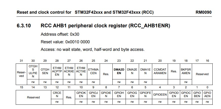
//Enable GPIOB clock
RCC->AHB1ENR |= 1UL<<1;
// Configuring PB6 and PB7 in Alternate function
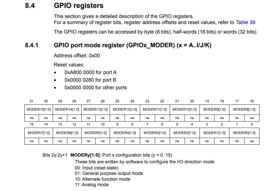
GPIOB->MODER |= ( (2UL<<(6*2)) | (2UL<<(7*2)) );
// Selecting PB6 and PB7 as Pull up pins
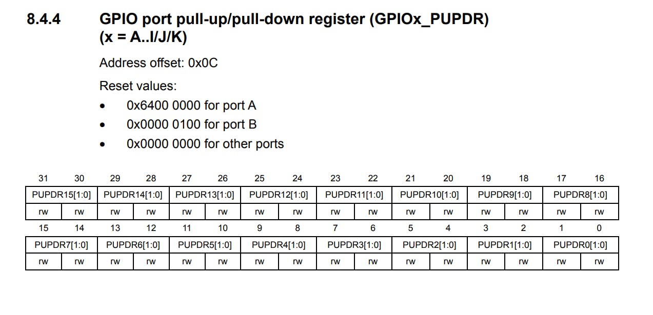
GPIOB->PUPDR |= ( (1UL<<(6*2)) | (1UL<<(7*2)));
// Setting PB6 and PB7 as open drain
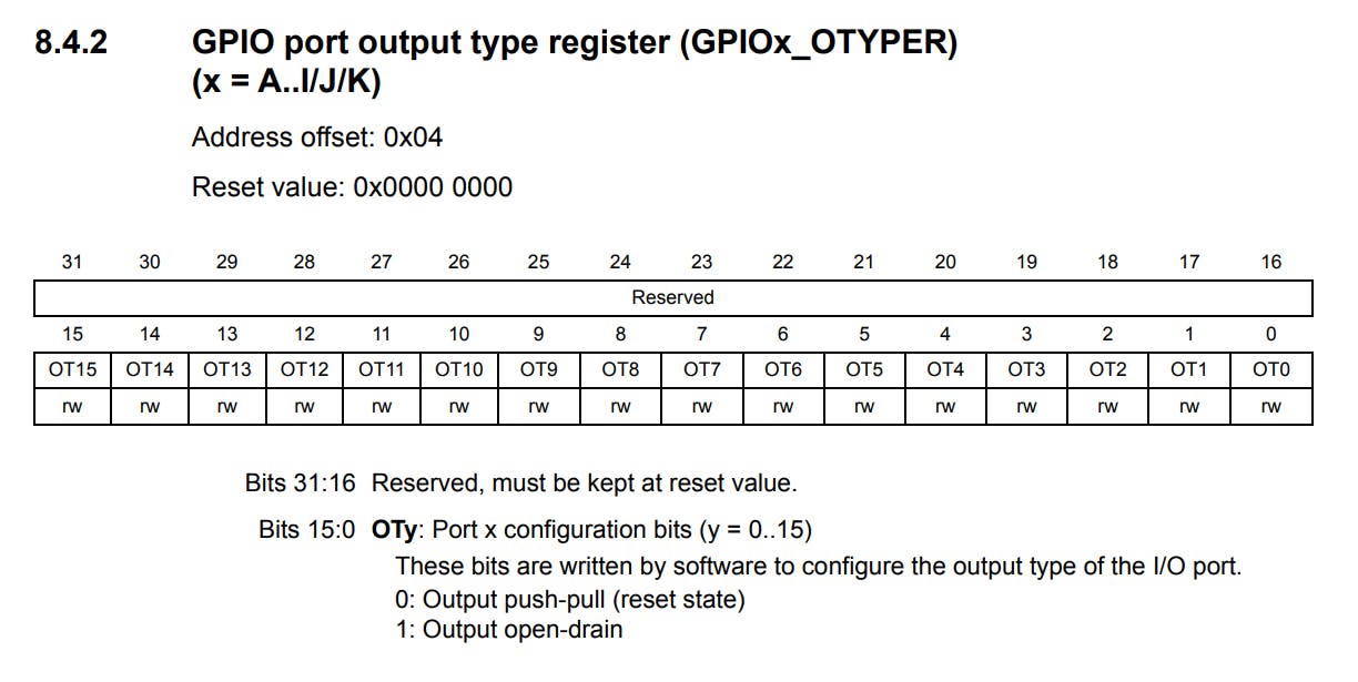
GPIOB->OTYPER |= ( (1UL<<6) | (1UL<<7) );
// Setting PB6 and PB7 at high speed
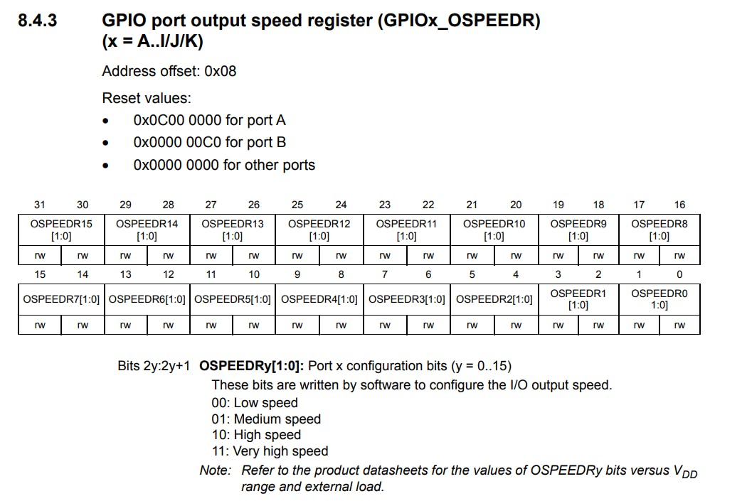
GPIOB->OSPEEDR |= ( (2UL<<(6*2)) | (2UL<<(7*2)) );
// Selecting the Alternate function (AF4)
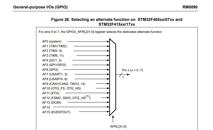
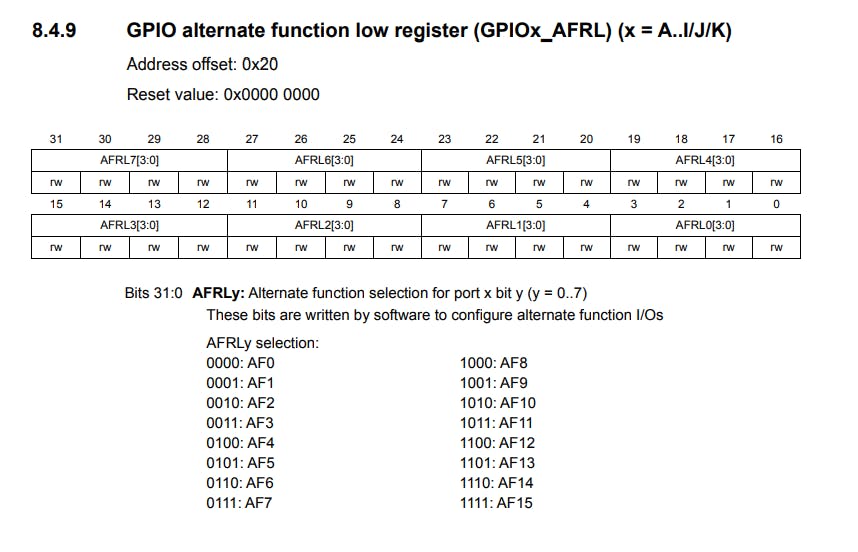
GPIOB->AFR[0] |= ( (4UL<<(6*4)) | (4UL)<<(7*4));
}
Here, since we will be using I2C1 we need to use PB6 and PB7 as can be seen from the above table. So, firstly the clock for the GPIOB port is enabled by writing a 1 to the GPIOBEN bit in the RCC->AHB1ENR register. Then, we set PB6 and PB7 in Alternate-Function mode by writing 10 to the MODER6[1:0] and the MODER7[1:0] bits in the GPIOB->MODER register.
After that, PB6 and PB7 need to be configured as pull-up pins and set as open drain for the I2C protocol. This is done by writing a 1 to the PUPDR6[1:0] and PUPDR7[1:0] bits in the GPIOB->PUPDR register. For the open-drain configuration, a 1 needs to written to the OT6 and the OT7 bits in the GPIOB->OTYPER register.
Then, we need to set PB6 and PB7 at High-Speed, to do this 10 is written to the OSPEEDR6[1:0] and the OSPEEDR7[1:0] bits in the GPIOB->OSPEEDR register. Finally, we need to select the alternate function that is AF4 for PB6 and PB7. This is done by writing a 0100 to the AFRL6[3:0] and the AFRL7[3:0] bits in the GPIOB->AFR[0] register.
- Now, the
I2C1Peripheral is initialized using thevoid I2C_Init()function,
void I2C_Init(){
// Enable I2C1 clock
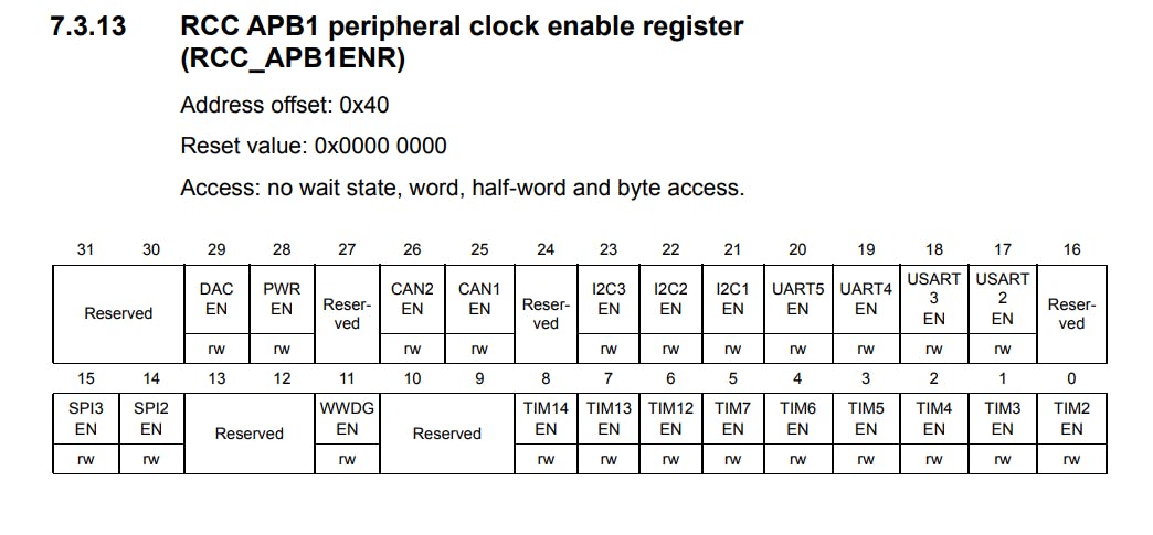
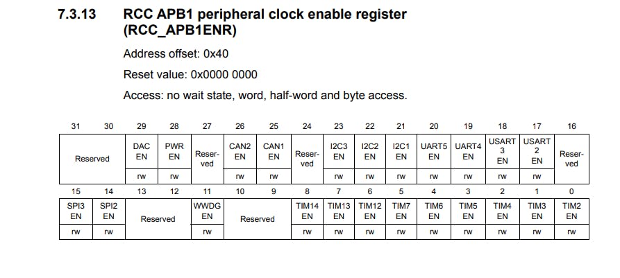
RCC->APB1ENR |= 1UL<<21;
// Reset I2C
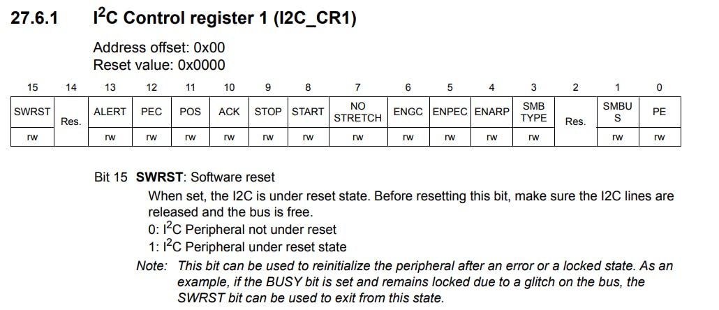
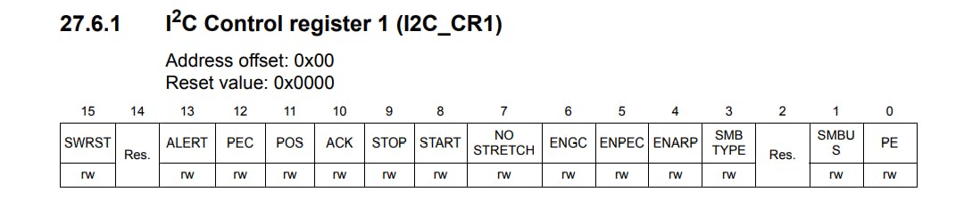
I2C1->CR1 |= 1UL<<15;
I2C1->CR1 &= ~(1UL<<15);
// Set I2C clock at 16MHz
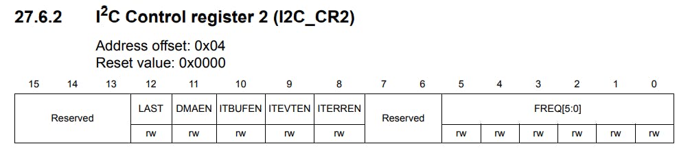
I2C1->CR2 |= 16UL<<0;
// Needs to be set high by software for I2C
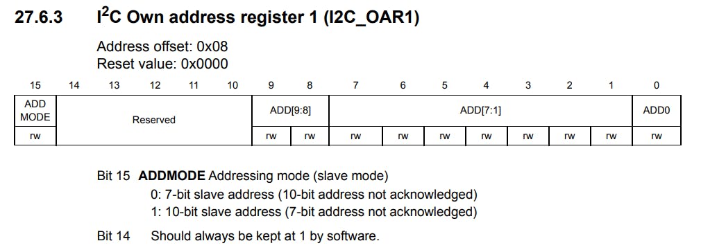
I2C1->OAR1 |= 1UL<<14;
// Set SCl at 100KHz
I2C1->CCR |= 0x50UL<<0;
// Configure rise time as 1000ns
I2C1->TRISE |= 17UL<<0;
// Enable I2C1
I2C1->CR1 |= 1UL<<0;
}
First, we enable the clock for I2C1 by writing a 1 to the I2C1EN bit in the RCC->APB1ENR register.
Then, we reset the I2C1 peripheral by first writing a 1 to the SWRST bit and then clearing it in the I2C1->CR1 register. After, that the I2C clock is set at 16 MHz by writing 16 to the FREQ[5:0] bits in the I2C1->CR2 register.
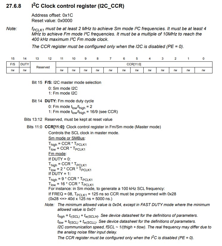
For the I2C Protocol the Bit 14 of the set HIGH by writing a 1 it in the I2C1->OAR1 register. After that, the SCL clock frequency and the Maximum Rise Time needs to be configured. The SCL frequency is set at 100 KHz by writing 0x50 to the CCR[11:0] bits in the I2C1->CCR register. This value is calculated as follows,
Since we want SCL to run at 100KHz, its time period will be :
$$ T = 1/F = 1/100KHz = 0.01 ms $$
And, we want the duty cycle to be 0.5, so the Ton will be :
$$ T_{on} = 0.01 ms / 2 = 0.005 ms = 5000 ns $$
Our peripheral clock is running at 16 MHz, so
$$ T_{PCLK} = 1 / F = 1 / 16 MHz = 62.5 ns $$
Therefore, the value that needs to be written in the CCR[11:0] bits can be found out by,
$$ CCR_{Value} = 5000 ns / 62.5 ns = 80 $$
The value 80 corresponds to 0x50 in Hexadecimal format. This value is then entered in the CCR[11:0] bits.
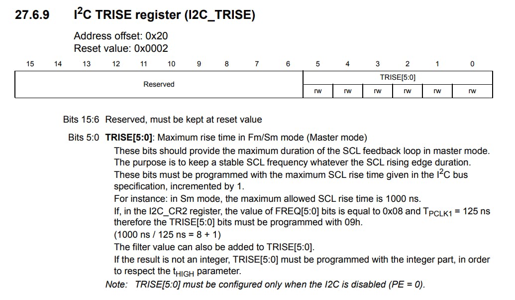
Then, we configure the Rise - Time to be 1000ns for the SCL. This is done by writing 17 to the TRISE[5:0] bits in the I2C1->TRISE register. Since our \(T_{PCLK} = 62.5 ns\), the value to be written in the TRISE[5:0] bits can be found out by,
$$ TRISE_{Value} = 1000 ns / 62.5 ns = 16 $$
And a 1 needs to be added to the above value while writing it to the register. Hence, we write the value 17.
Finally, we enable the I2C peripheral by writing a 1 to the PE bit in the I2C1->CR1 register.
- After that, now we move on to the
void I2C_Start()function,
void I2C_Start(){
// Enable the acknowledgment ACK bit
I2C1->CR1 |= 1UL<<10;
// Set the START bit to Start Communication
I2C1->CR1 |= 1UL<<8;
// SB bit is set when START condition is generated
// So, it is polled to make sure communication has started
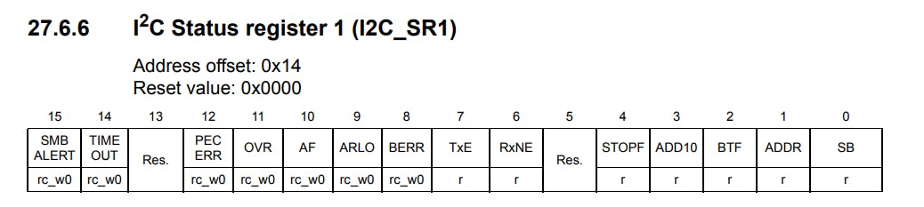
while(!(I2C1->SR1 & I2C_SR1_SB)){}
}
By using this function we can start the I2C Communication. To do this, first, we enable the acknowledgment bit in the I2C1->CR1 register by writing a 1 to its ACK bit. Then, we set the START bit to 1 in the I2C1->CR1 register to enable Repeated Start Condition Generation.

Whenever a Start condition is generated the SB bit is set to 1 in the I2C1->SR register by the Hardware. So, we poll it to make sure that the communication is started.
- Then, we have the
void I2C_Write(uint8_t var)function,
void I2C_Write(uint8_t var){
    // Polling the TxE bit in the I2C_SR1 register to see if
    // data register is empty
    while(!(I2C1->SR1 & I2C_SR1_TXE)){}

    // Put the data to be written in the I2C_DR register
    I2C1->DR = var;

    // Poll the BTF (Byte Transfer Finished) bit in the I2C_SR1 register to confirm
    // Byte transfer
    while(!(I2C1->SR1 & I2C_SR1_BTF)){}
}
Firstly, the TXE bit of the I2C1->SR register is polled to check whether the data register is empty. Once, that's done we assign the I2C1->DR register the value given to us by the user, which is var in this case. Then, we make sure that the Byte Transfer is finished by polling the BTF bit in the I2C1->SR register.

- For sending the slave device address we use the
void I2C_Send_Addr(uint8_t Addr)function,
void I2C_Send_Addr(uint8_t Addr){
    //Put the address to be sent into the I2C_DR register
    I2C1->DR = Addr;

    // ADDR bit is polled in the I2C_SR1 register for end of
    // address transmission
    while(!(I2C1->SR1 & I2C_SR1_ADDR)){}

    // Variable that will read I2C_SR1 and I2C_SR2
    // for clearing the ADDR bit
    clc = (I2C1->SR1 | I2C1->SR2);
}
Here, the Address given by the user which is Addr in this case is assigned to the I2C1->DR register. Then by polling the ADDR bit in the I2C1->SR register, we confirm that the address has been sent successfully. To clear the ADDR bit, we need to read the I2C1->SR1 and I2C1->SR2 registers. Here, our user-defined variable clc will come into the picture. We use it to read these registers so that the ADDR bit is cleared.
- To stop the I2C communication the
void I2C_Stop()function is used,
void I2C_Stop(){
    // Stop Communication after current byte transfer
    I2C1->CR1 |= 1UL<<9;
}
Here, we just need to write a 1 to the STOP bit in the I2C1->CR1 register to stop the communication.
- Now, we need to send the commands to the LCD to initialize it or instruct it do something, once initialization is done, for that we use the
void LCD_Write_Cmd(uint8_t Device_Addr,uint8_t Slave_Reg_Addr, uint8_t data)function,
void LCD_Write_Cmd(uint8_t Device_Addr,uint8_t Slave_Reg_Addr, uint8_t data){
    uint8_t d_h, d_l, d1, d2, d3, d4;
    d_h = data & 0xF0;
    d_l = (data << 4) & 0xF0;

    // Set EN = 1 and RS = 0 and R/W =0 for writing to
    // Instruction Register and send the Upper 4 bits
    d1 = d_h | 0x0C;
    d2 = d_h | 0x08; // Set EN = 0 and RS = 0 and set Back Light on

    // Set EN = 1 and RS = 0 and R/W = 0
    // for Instruction Register and send the Lower 4 bits
    d3 = d_l | 0x0C;
    d4 = d_l | 0x08; // Set EN = 0 and RS = 0 and set Back Light on

    I2C_Start();
    I2C_Send_Addr(Device_Addr);
    I2C_Write(Slave_Reg_Addr);
    I2C_Write(d1);
    TIM4_ms_Delay(2); // Wait for 2 ms for the command to take action
    I2C_Write(d2);
    I2C_Write(d3);
    TIM4_ms_Delay(2); // Wait for 2 ms for the command to take action
    I2C_Write(d4);
    I2C_Stop();
}
Here, we declare some variables inside our function, since we will need to extract the higher and lower 4-bits from the data and transmit them. To extract the higher 4-bits we use the Bitwise AND operation, that is data & 0xF0. For the lower four bits we use the logical shift left operation and then do the bitwise AND, that is (data << 4) & 0xF0. Now, that we have our lower and upper bits, we need to write this to the LCD. To write any data to the LCD a pulse of a specific duration needs to be sent to the EN pin of the LCD. Let's bring up the connection table we saw earlier that described the PCF8574T and the 16x2 LCD connections.
| PCF8574T | 16x2 LCD |
| P0 | RS |
| P1 | R/W |
| P2 | EN |
| P3 | Back Light |
| P4 | D4 |
| P5 | D5 |
| P6 | D6 |
| P7 | D7 |
As seen from the above table, we can infer that P0-P3 are our control pins for the LCD, and P4-P7 are our data pins. So we need to manipulate the state of the control pins to be able to write anything to our LCD. To do this, we use the bitwise OR operation, that is d_h | 0x0C. To understand this, let's consider an example.
Let d_h = 0101 0000
Mask = 0x0C = 0000 1100
After the bitwise OR operation, we get,
d_h | Mask = 0101 1100
Now, let's map these bits to the P0-P7 pins,
| PCF8574T | 16x2 LCD | Transmitted Value |
| P0 | RS | 0 |
| P1 | R/W | 0 |
| P2 | EN | 1 |
| P3 | Back Light | 1 |
| P4 | D4 | 1 |
| P5 | D5 | 0 |
| P6 | D6 | 1 |
| P7 | D7 | 0 |
From the above table, we can see that the data is successfully mapped to the P4-P7 or data pins, and the control bits are changed. The EN bit is set HIGH, the instruction register is selected since RS bit is 0, and write operation is performed because R/W bit is 0. Now, to send a pulse we need to wait for some time and then set the EN bit to zero (We will see this soon in the I2C transmission cycle). So, each of 4-bits need to be sent twice. Hence, we require the Burst Write Sequence. While sending the same data again we set the EN bit to 0, and let the backlight remain on by setting P3 to 1. This is done by bitwise OR operation with 0x08. This procedure is repeated again for the lower four bits.
Now, let's see the I2C transmission cycle by following the I2C frame. We call the I2C_Start() function, to generate the Start condition. After that send the Slave device address using I2C_Send_Addr(Device_Addr). To determine where the write operation needs to performed on the slave device we send the slave register address by calling I2C_Write(Slave_Reg_Addr). Then, we send our upper 4-bits by calling I2C_Write(d1). After that, we wait for 2ms by calling our delay function TIM4_ms_Delay(2). This is done to create that pulse on the EN pin as we talked about above. Then, we send the upper 4-bits again. Similarly, all the data is sent. After that, we end the transmission cycle by calling I2C_Stop().
- The
void LCD_Write_Data(uint8_t Device_Addr, uint8_t Slave_Reg_Addr, uint8_t data)function is very similar to the function above, the only difference is here we select the Data Register of the LCD by writing a1to theRSbit. This is done by thebitwise ORoperation as described earlier.
void LCD_Write_Data(uint8_t Device_Addr, uint8_t Slave_Reg_Addr, uint8_t data){
    uint8_t d_h, d_l, d1, d2, d3, d4;
    d_h = data & 0xF0;
    d_l = (data << 4) & 0xF0;

    // Set EN = 1 and RS = 1 and R/W = 0 for writing to
    // Data Register and send the Upper 4 bits
    d1 = d_h | 0x0D;
    d2 = d_h | 0x09; // Set EN = 0 and RS = 1 and set Back Light on

    // Set EN = 1 and RS = 1 and R/W = 0 for writing to
    // Data Register and send the Lower 4 bits
    d3 = d_l | 0x0D;
    d4 = d_l | 0x09; // Set EN = 0 and RS = 1 and set Back Light on

    I2C_Start();
    I2C_Send_Addr(Device_Addr);
    I2C_Write(Slave_Reg_Addr);
    I2C_Write(d1);
    TIM4_ms_Delay(2); // Wait for 2 ms for the data to be written
    I2C_Write(d2);
    I2C_Write(d3);
    TIM4_ms_Delay(2); // Wait for 2 ms for the data to be written
    I2C_Write(d4);
    I2C_Stop();
}
- Then for setting the LCD cursor at a specific position we use the
void LCD_Cursor(int r, int c)function,
void LCD_Cursor(int r, int c){
    if (r==1){
        c |= 0xC0;
        LCD_Write_Cmd(LCD_ADDR, INST_REG, c);
    }
    else{
        c |= 0x80;
        LCD_Write_Cmd(LCD_ADDR, INST_REG, c);
    }
}
To set the cursor, we take in the arguments for the row and column by the user. The starting address for the first cell of the LCD on the first row is 0x80, and the address for the first cell on the second row is 0xC0. So, we check the row number and according to it determine the cell that the user wants the cursor on by using the bitwise OR operation. Then, we call the LCD_Write_Cmd(LCD_ADDR, INST_REG, c) function and pass into it the LCD address, the Instruction Register address on the LCD, and our answer from the bitwise OR operation.
- To initialize and configure the LCD we use the
void LCD_Init()function,
void LCD_Init(){
    // 1. Initializing the LCD in 4-bit mode
    TIM4_ms_Delay(50);
    LCD_Write_Cmd(LCD_ADDR,INST_REG,0x30);
    TIM4_ms_Delay(5);

    LCD_Write_Cmd(LCD_ADDR,INST_REG,0x30);
    TIM4_ms_Delay(1);

    LCD_Write_Cmd(LCD_ADDR,INST_REG,0x30);
    TIM4_ms_Delay(10);

    LCD_Write_Cmd(LCD_ADDR,INST_REG,0x20); // Set the LCD in 4-bit Mode
    TIM4_ms_Delay(10);

    // 2. Initializing the Display

    // Function Set (DL=0 for 4-bit mode; N=1 for 2-line display;
    // F=0 for 5x8 characters)
    LCD_Write_Cmd(LCD_ADDR,INST_REG,0x28);
    TIM4_ms_Delay(5);

    // Display Control (D=0;C=0;B=0 - Display is off)
    LCD_Write_Cmd(LCD_ADDR,INST_REG,0x08);
    TIM4_ms_Delay(5);

    // Clear the display
    LCD_Write_Cmd(LCD_ADDR,INST_REG,0x01);
    TIM4_ms_Delay(5);

    TIM4_ms_Delay(1); // Wait for some time

    // Set Entry Mode (ID=1 for incrementing cursor and S=0 for no shift)
    LCD_Write_Cmd(LCD_ADDR,INST_REG,0x07);
    TIM4_ms_Delay(5);

    // Display Control (D=1;C=0;B=0 - Cursor blinks)
    LCD_Write_Cmd(LCD_ADDR,INST_REG,0x0F);
    TIM4_ms_Delay(5);
}
This is a standard initialization procedure that needs to be performed while using the 16x2 LCD module. This configuration is done based on the table below, and the delay after each instruction is provided based on its execution time.
- For our delay, we use
TIM4in thevoid TIM4_ms_Delay(uint16_t delay)function,
void TIM4_ms_Delay(uint16_t delay){
RCC->APB1ENR |= 1<<2; //Start the clock for the timer peripheral
TIM4->PSC = 16000-1; //Setting the clock frequency to 1kHz.
TIM4->ARR = (delay); // Total period of the timer
TIM4->CNT = 0;
TIM4->CR1 |= 1; //Start the Timer
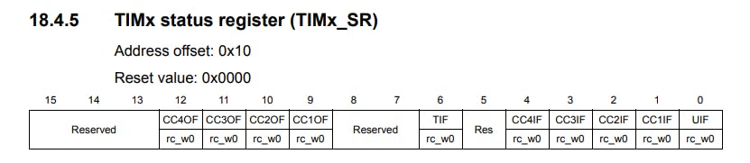
while(!(TIM4->SR & TIM_SR_UIF)){} //Polling the update interrupt flag
TIM4->SR &= ~(0x0001); //Reset the update interrupt flag
}
Here, we enable the clock for the Timer 4, and set the Pre-scalar to 16000-1 to reduce the clock speed to 1 KHz, which means one clock tick corresponds to 1ms. After that, we assign the desired delay value to the TIM2->ARR register, initialize the count to zero and start the timer. Then we poll the UIF or the Update Interrupt Flag, which is set after the desired amount of clock ticks provided in the TIM2->ARR register are done, or in other words when the timer overflows. After the UIF flag is set we clear it from the TIM2->SR register and exit the function.
6. Writing our main function
int main(void){
    GPIO_Init();
    I2C_Init();
    LCD_Init();
    LCD_Cursor(0,0); // Set the cursor at the first row and first column
    LCD_Write_Data(LCD_ADDR,DATA_REG, 0x84); // Character Generation ROM Pattern for 'H'
    LCD_Write_Data(LCD_ADDR,DATA_REG, 0x54); // Character Generation ROM Pattern for 'E'
    LCD_Write_Data(LCD_ADDR,DATA_REG, 0xC4); // Character Generation ROM Pattern for 'L'
    LCD_Write_Data(LCD_ADDR,DATA_REG, 0xC4); // Character Generation ROM Pattern for 'L'
    LCD_Write_Data(LCD_ADDR,DATA_REG, 0xF4); // Character Generation ROM Pattern for '0'
    TIM4_ms_Delay(1000); // Delay of 1s
    while(1){ // Dead Loop
    }
}
In our main function, we first call all our initialization functions, which we GPIO_Init(), I2C_Init() and LCD_Init() . Then, we set the LCD cursor at the first cell in the first row, by calling the LCD_Cursor(0,0) function and passing it a 0 for both the row and column values. Then we call the LCD_Write_Data function and pass it the LCD address, the Data register address on the LCD, and the CGROM code for each character of the string HELLO. Then we, enter a dead while loop. There you go, the word HELLO is successfully displayed on the LCD screen 😄.
Conclusion
That marks the end of our I2C Protocol tutorial. This article covered the basics of this communication protocol. But we have not covered the read cycle of the I2C Protocol here, because in this case, we did not need to read anything from the LCD. This can also be done easily by following the steps above, the only change that needs to be done is that the LSB of our address field should be 1, to specify that we desire to read data from our slave device.
I hope you found this article useful and easy to follow along😀. All the codes used here are present in my GitHub repository, which you can access by clicking here.
And, the demo video for this tutorial can be found here.

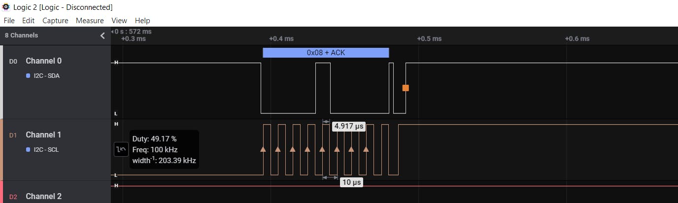
The pictures below show the various parts of a single I2C Frame captured through a logic analyzer.