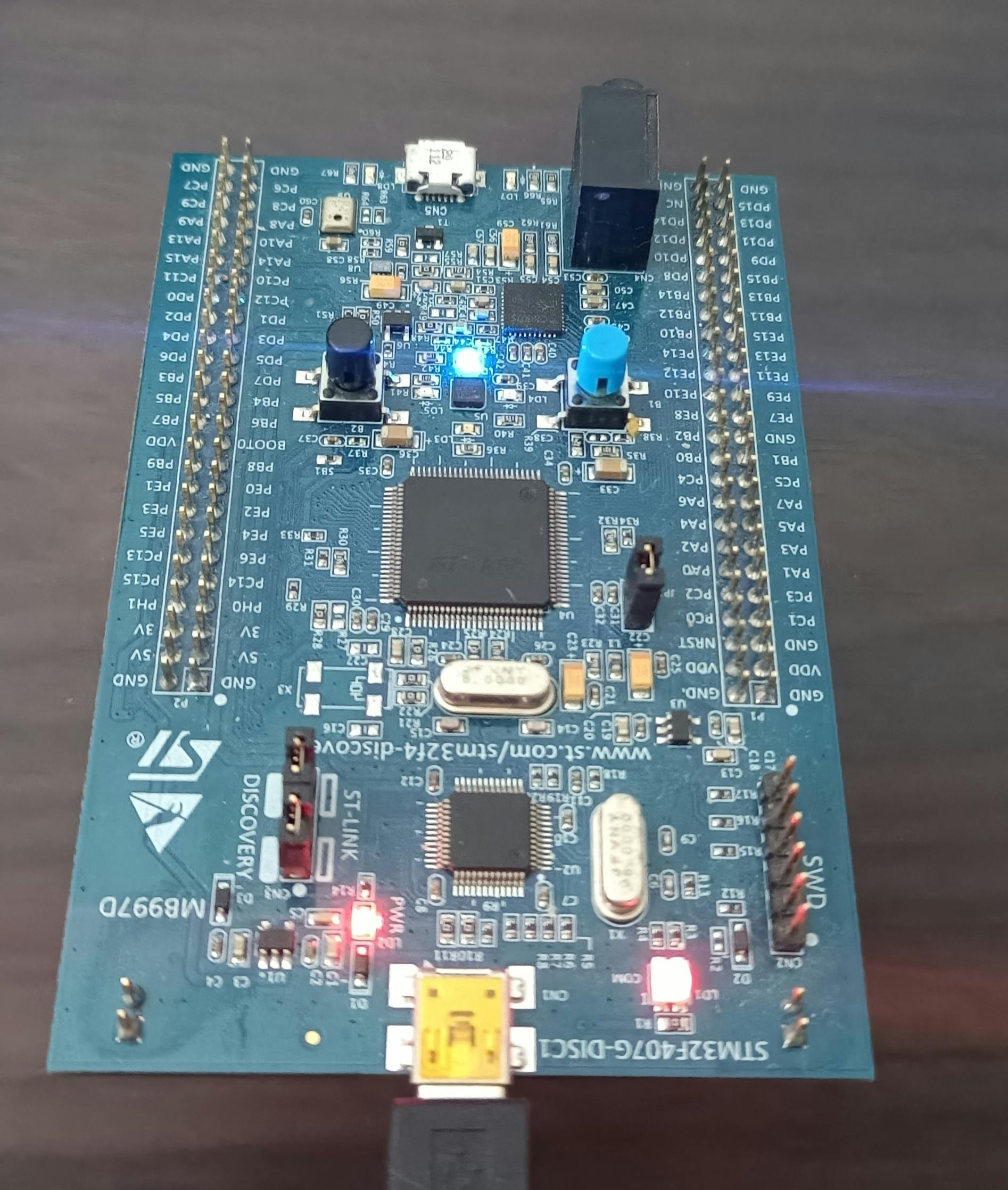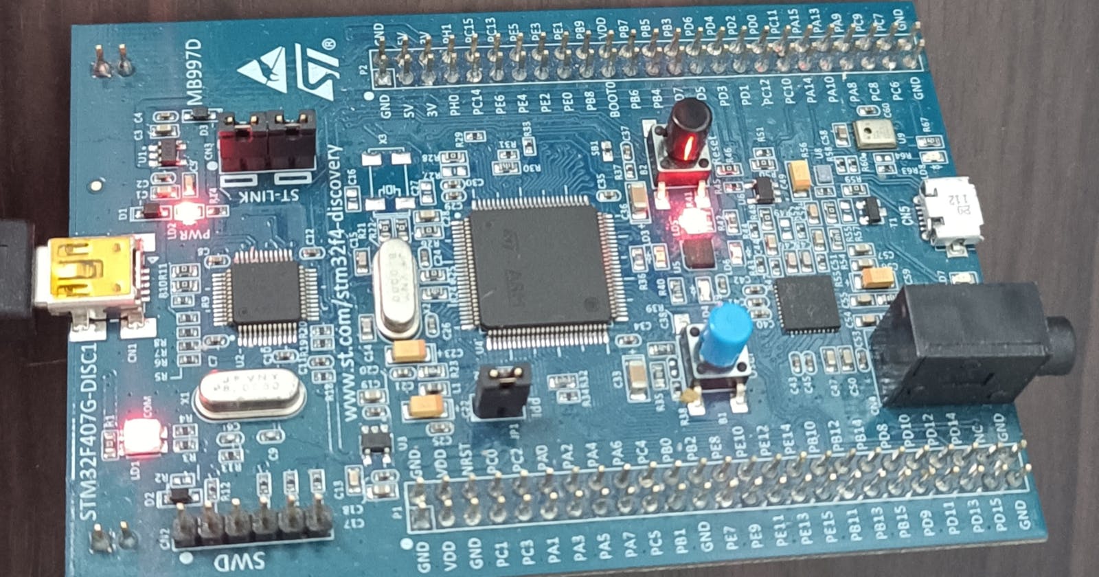
Interfacing LIS302DL Accelerometer using the SPI Protocol with the STM32F407VG-DISC1 Development Kit


Introduction
Hi! 😄, I am here yet again with a new project. This time we will be interfacing the on-board LIS302DL MEMS Accelerometer with our STM32F407 Development Board. Accelerometers as we all know are used everywhere in our daily lives. Some of the places where they play a major role are smartphones, wearable devices, etc. They have a vast number of applications in various fields including but not limited to industries like the Biomedical, Space Navigation, and Defence. So, the skill required to program them becomes important. Another added advantage is to learn about the SPI Protocol, which is also one of the dominant concepts in Embedded Systems. Now, that we have enough motivation, let's proceed to understand some of the underlying ideas in this project.
Working Principle

Since an external module is not in use here (as I explained earlier that the STM32F407VG-DISC1 has this sensor onboard), we do not need to make any physical(manual) connections as such. But, we do need to look at the schematic for the sensor to figure out which pins are mapped to which of the predefined wires of SPI. So, before going into that, let's take a brief look at the SPI(Serial Peripheral Interface) Protocol, and how it works.
SPI is a synchronous, full-duplex, master-slave-based, serial communication protocol. The synchronous aspect implies that a common clock is used by the slave and the master to perform operations, and this clock is generated and sent by the master to the slave. Full-Duplex suggests that communication between the devices can happen at the same time, i.e. data can be sent and received by the master and slave simultaneously. As you might have noticed by now it operates based on master-slave-based communication, i.e. the master controls the communication between itself and multiple slaves. The SPI protocol uses a shift register type mechanism. To exemplify, when a value is written to a specific register in the slave, the previous value is pushed out and communicated with the master. This makes SPI serial in nature.
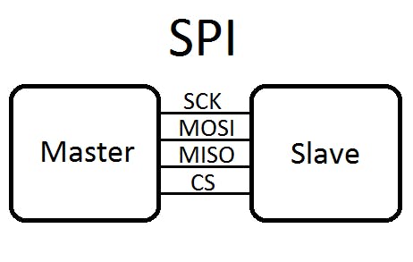
As seen from the figure above, SPI communication is generally a 4-wire (3-wire communication is also possible) based protocol. These are namely SCK (Serial Clock), MISO (Master-In Serial-Out), MOSI (Master-Out Serial-In), and CS (Chip-Select). Unlike, I2C there is no address-based communication here, instead here, as the name implies, the CS pin is used to communicate between the Master and a particular Slave. So, whenever data exchange between the master and a particular slave needs to be initiated, the CS pin connected to that slave is pushed to 0 by the master. One of the most important parts of this protocol is configuring CPOL and CPHA parameters, which stand for Clock Polarity and Clock Phase respectively. The clock polarity parameter is used for the idle state of the clock, i.e. if this is set to 0, it implies that the clock remains at 0, when idle, and the clock phase determines the edge of the clock on which data is sampled, i.e. when this is set to 0, the data sampling is done of the first edge of the clock, after the idle state.
| CPOL | CPHA | Configuration |
| 0 | 0 | The clock remains at 0 when idle and the data sampling is done at the first edge, i.e. the rising edge. |
| 0 | 1 | The clock remains at 0 when idle and the data sampling is done at the second edge, i.e. the falling edge. |
| 1 | 0 | The clock remains at 1 when idle and the data sampling is done at the first edge, i.e. the falling edge. |
| 1 | 1 | The clock remains at 1 when idle and the data sampling is done at the second edge i.e. the rising edge. |
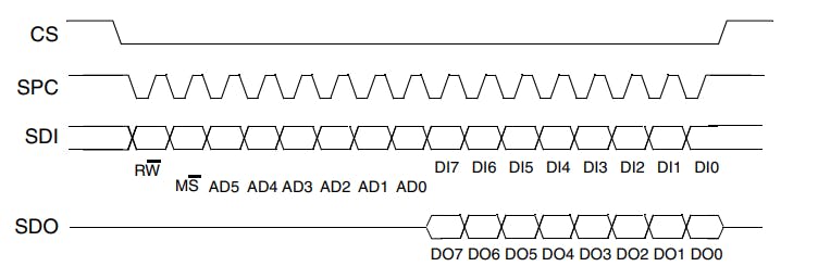
The table above shows all the possible configurations for CPOL and CPHA. The figure below shows an example timing diagram for a particular configuration of the SPI protocol. As can be seen, the clock is at 1 when idle, which implies CPOL=1, and the data is sampled at the second edge of the clock, meaning CPHA=1. Let's analyze the timing diagram, first, we push theCS pin to 0, therefore establishing a link with a particular slave. Then, as just discussed as per CPOL and CPHA data is sampled. After that, first, the address of the register on the slave that needs to be accessed is sent, and then the actual data is sent. The first bit of the address signifies whether a read or write operation needs to be performed. So, if a 1 is sent as the first bit of the address, it suggests that a read operation needs to be performed and vice-versa. Also, notice how, as the data is sent via the MOSI(SDI) line, immediately data is pushed onto the MISO(SDO) line. This is due to the shift register mechanism employed in SPI.
Now, that we have enough understanding of the SPI protocol, let's move on to the project. Today, we will be using the values obtained from the accelerometer to toggle LEDs on our board, which will create a sort of gravity effect.
Before jumping into programming, remember I said that we will need to look at the schematics, well now is the time for that.
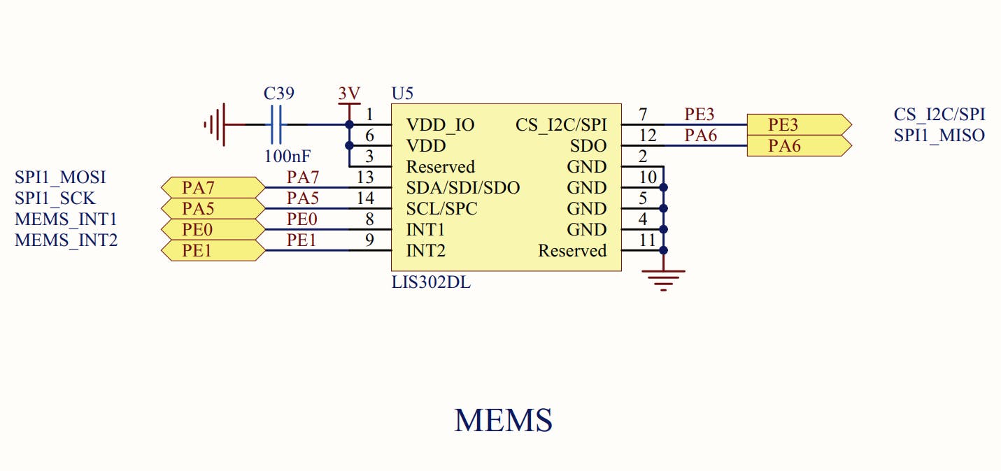
The schematic shows that CS is connected to PE3, SPI1_SCK is connected to PA5, SPI1_MISO is connected to PA6, and SPI1_MOSI is connected to PA7. So, we will need to keep this in mind, while configuring the GPIO pins. Also, notice how it says SPI1 everywhere, this is because there are 3 SPIs available on the STM32F407, and the MEMS sensor is connected to SPI1. Hence, we will program SPI1. The MEMS_INT1 and MEMS_INT2 pins are used when interrupts are being used, for today, we will not be looking at them. Note that this sensor works with I2C as well.
On a side note, all the code and the datasheet for LIS302DL used here will be available in my GitHub repo, which can be accessed by clicking here.
Components Required
An STM32F407VG-DISC1 development board or other STM32F4-based development boards can also be used if they have the onboard LIS302DL MEMS accelerometer.
A Logic Analyzer.
A few jumper wires to connect to the Logic Analyzer.
So, pull out your dev kits everyone, and let's start coding!
Programming the STM32F407
We will be using register-level programming for this as always. Let's start by including the necessary header files.
1. Including the Header Files
/******************************************************************************
 * This is the register-level code for interfacing the on-board LIS302DL
 * accelerometer using the SPI Protocol.
 *
 * Configurations are as follows:
 * CS        - PE3
 * SCK       - PA5
 * MOSI      - PA7
 * MISO      - PA6
 *
 * @File     main.c
 * @Author   Ruturaj A. Nanoti
 *
 *****************************************************************************/

#include "stm32f4xx.h"
#define ARM_MATH_CM4
These are the header files included at the top of our main.c file. The stm32f4xx.h is the one for our microcontroller and the ARM_MATH_CM4 is for any math operations that we perform in our code.
2. Defining Register Addresses for LIS302DL
//Register Definitions for LIS302DL
#define LIS302DL_ADDR     (0x3B)
#define WHO_AM_I          (0x0F)
#define CTRL_REG1         (0x20)
#define CTRL_REG2         (0x21)
#define CTRL_REG3         (0x22)
#define HP_FILTER_RESET   (0x23)
#define STATUS_REG        (0x27)
#define OUT_X             (0x29)
#define OUT_Y             (0x2B)
#define OUT_Z             (0x2D)
These are the addresses of various registers of the accelerometer that we are using, obtained from the datasheet.
3. Defining Calibration Constants
// Calibration constants
#define X_OFFSET 18
#define THRESH_LOW -120
#define THRESH_HIGH 120
Some of the calibration parameters and thresholds are defined here, this will become clear as and when we progress further.
4. Declaring the User-Defined Functions and variables
//User-defined Function Declarations
void RCC_Init(void);
void GPIO_Init(void);
void SPI_Init(void);
uint16_t SPI_Transmit(uint8_t data);
uint16_t SPI_Receive(uint8_t addr);
void LIS_Init(void);
void LIS_Write(uint8_t addr, uint8_t data);
void LIS_Read(void);
int16_t Convert_To_Val(uint16_t val);
void TIM4_ms_Delay(uint16_t delay);

//User-defined variables
uint16_t x,y,z;
int16_t x_final, y_final, z_final;
uint16_t rxd,rxdf;
The functions used in the code are declared here. The void GPIO_Init(void) and void SPI_Init(void) are used to initialize and configure the GPIO pins and SPI1 respectively. Then, we have the uint16_t SPI_Transmit(uint8_t data) and uint16_t SPI_Receive(uint8_t addr) functions, which are used to transmit and receive data on the SPI. The accelerometer-related functions are void LIS_Init(void), void LIS_Write(uint8_t addr, uint8_t data) and void LIS_Read(void), which initialize LIS302DL, write data to it, and read data from it respectively. Finally, the int16_t Convert_To_Val(uint16_t val) and void TIM4_ms_Delay(uint16_t delay) functions are used to process the raw data, and create delay in milliseconds using TIM4.
5. Defining the User-Defined Functions
- Initializing and Configuring the GPIO Pins with
GPIO_Init(),
void GPIO_Init(){
// Enable GPIOA clock
RCC->AHB1ENR |= RCC_AHB1ENR_GPIOAEN;
// Configuring PA5, PA6, PA7 in alternate function mode
GPIOA->MODER |= (GPIO_MODER_MODER5_1 | GPIO_MODER_MODER6_1 | GPIO_MODER_MODER7_1);
// Select AF5 for SPI on PA5, PA6, PA7
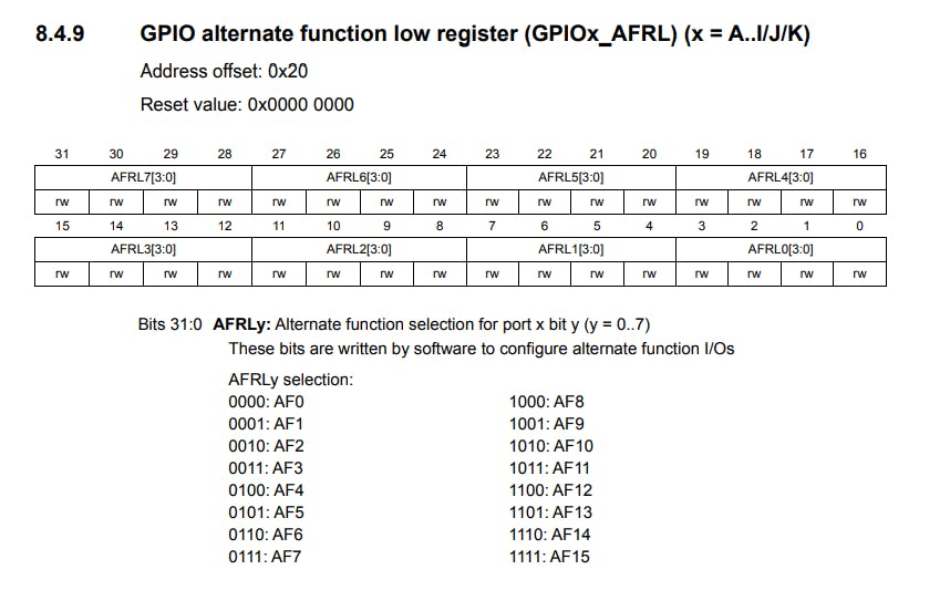
GPIOA->AFR[0] |= (GPIO_AFRL_AFSEL5_2 | GPIO_AFRL_AFSEL5_0
| GPIO_AFRL_AFSEL6_2 | GPIO_AFRL_AFSEL6_0
| GPIO_AFRL_AFSEL7_2 | GPIO_AFRL_AFSEL7_0);
// Enable GPIOE clock
RCC->AHB1ENR |= RCC_AHB1ENR_GPIOEEN;
// Since PE3 is CS, it needs to be configured in Output Mode
GPIOE->MODER |= GPIO_MODER_MODER3_0;
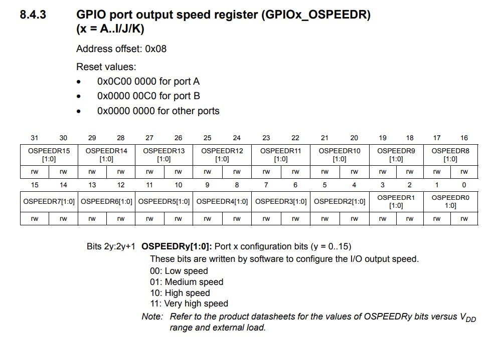
GPIOA->OSPEEDR |= ( GPIO_OSPEEDER_OSPEEDR5_0 | GPIO_OSPEEDER_OSPEEDR6_0 |
GPIO_OSPEEDER_OSPEEDR7_0);
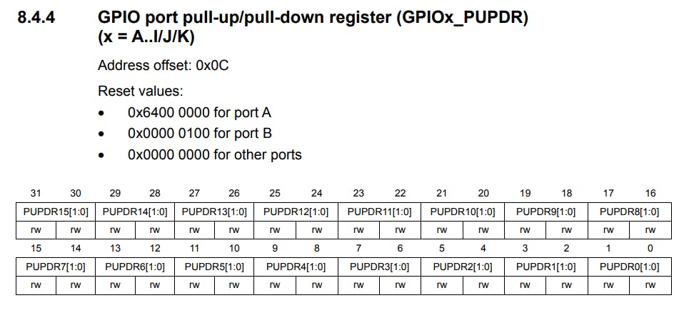
GPIOA->PUPDR |= (GPIO_PUPDR_PUPD5_1 | GPIO_PUPDR_PUPD6_1 | GPIO_PUPDR_PUPD7_1);
// Enable clock for GPIOD and Configure PD12 in output mode
RCC->AHB1ENR |= RCC_AHB1ENR_GPIODEN;
GPIOD->MODER |= (GPIO_MODER_MODER12_0 | GPIO_MODER_MODER13_0 | GPIO_MODER_MODER14_0 | GPIO_MODER_MODER15_0);
}
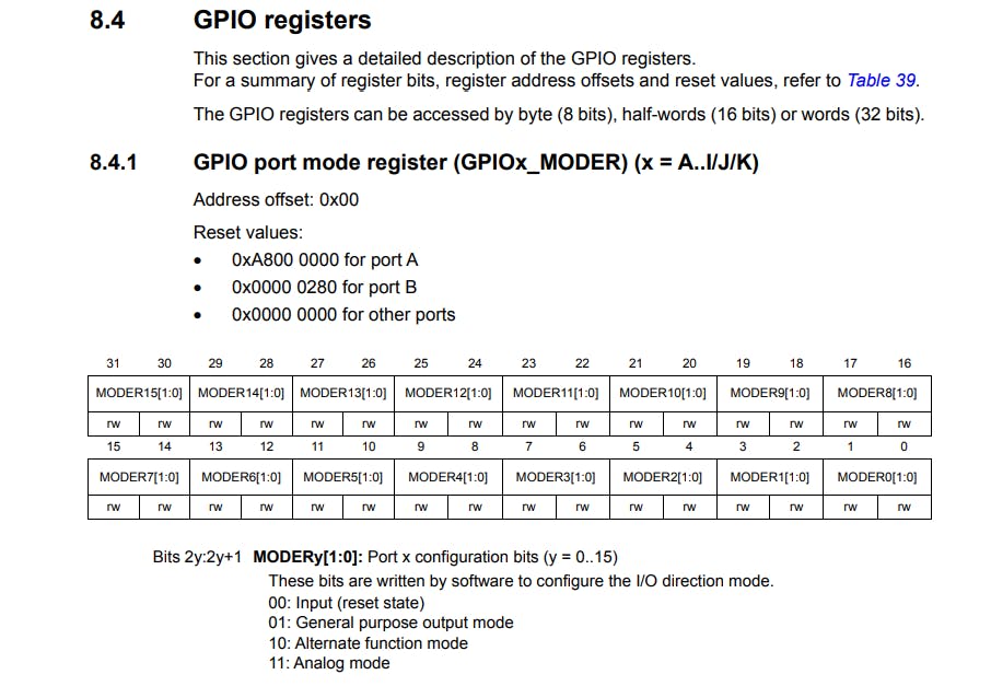
Firstly, we enable GPIOA port, by writing a 1 to position 0 in the RCC->AHB1ENR register. Then, PA5, PA6, and PA7 need to be put into Alternate Function (AF) mode. This is done by writing 10 to positions 10, 12, and 14 in the GPIOA->MODER register.
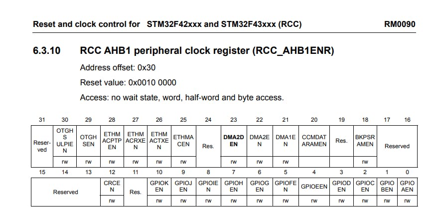
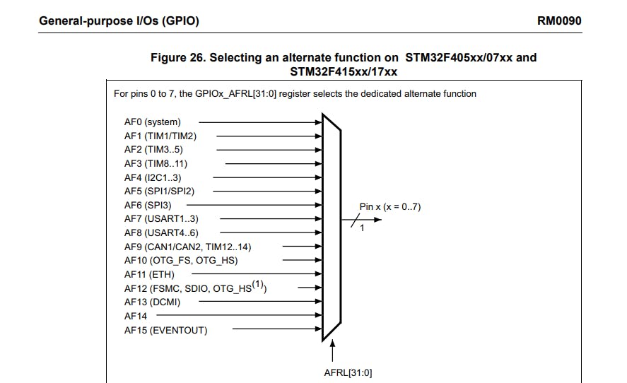
For using SPI1, we need to use AF5, we do that by writing 101 to positions 20, 24, and 28 in the GPIOA->AFR[0] register.
After that, we configure PE3 to be in output mode, which is done by first enabling the GPIOE clock. This is accomplished by writing a 1 to position 4 in the RCC->AHB1ENR register. PE3 is put into output mode by writing a 1 to position 6 in the GPIOE->MODER register. Then PA5, PA6, and PA7 are configured to run at medium speed by writing a 1 at positions 10, 12, and 14 in GPIOA->OSPEEDR register. This is followed by writing 10 to positions 10, 12, and 14 in GPIOA->PUPDR register, which puts PA5, PA6, and PA7 in Pull-Down mode.
Finally, all the pins connected to 4 LEDs on the development kit are configured in output mode. For this, first, we enable GPIOD clock, by writing a 1 to position 3 in RCC->AHB1ENR register. Then, PD12, PD13, PD14, and PD15 are set in output mode by writing a 1 to positions 24, 26, 28, and 30 in the GPIOD->MODER register.
- Setting up SPI with
void SPI_Init()function,
void SPI_Init(){
    // Enable SPI clock
    RCC->APB2ENR |= RCC_APB2ENR_SPI1EN;

    // Select the Master Configuration
    SPI1->CR1 |= SPI_CR1_MSTR;

    SPI1->CR1 &= ~SPI_CR1_BIDIMODE;

    SPI1->CR1 &= ~SPI_CR1_RXONLY;

    // Set the Data Frame Format (DFF) to '0' or 8-bit.
    SPI1->CR1 &= ~SPI_CR1_DFF;

    // SSI and SSM bits in the SP1->CR1 register need to be set
    // to '1'
    SPI1->CR1 |= (SPI_CR1_SSI | SPI_CR1_SSM);

    // Setting Baud Rate
    SPI1->CR1 &= ~SPI_CR1_BR;

    // Set the transmission to MSB First Mode
    SPI1->CR1 &= ~SPI_CR1_LSBFIRST;

    // Configure CPOL and CPHASE to '0' and '0', respectively.
    // i.e. Clock is at '0' when idle, and data capture is done
    // on the first clock transition which is the rising edge.
    SPI1->CR1 &= ~SPI_CR1_CPHA;
    SPI1->CR1 &= ~SPI_CR1_CPOL;

    // Enable CRC
    SPI1->CR1 |= SPI_CR1_CRCEN;

    // Enable SPI
    SPI1->CR1 |= SPI_CR1_SPE;

    // Selecting Motorola Format
    SPI1->CR2 = 0x0000;
}
First, we need to enable the clock for SPI, by writing a 1 to position 12 in the RCC->APB2ENR register. After that, the STM32F407 needs to be configured as a master for that, we write a 1 to position to 2 in the SPI1->CR1 register. Then, we disable the bidirectional-data mode and receive only (i.e. enable full-duplex mode). We do this by writing a 0 at positions 15 and 10 in the SPI1->CR1 register.
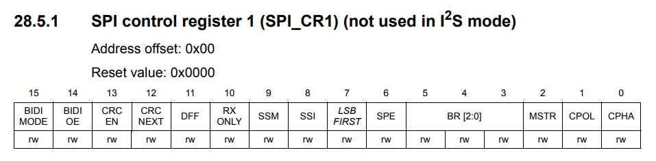
Now, the 8-bit data format is selected, by writing a 0 to position 11 in the SPI1->CR1 register. Then, the SSI and SSM(Software Slave Management) bits need to be set to 1 for SPI in the SPI1->CR1 register. Following this, we set the Baud rate to be,
$$BR=f_{PCLK}/2$$
where,
$$f_{PCLK}=16MHz$$
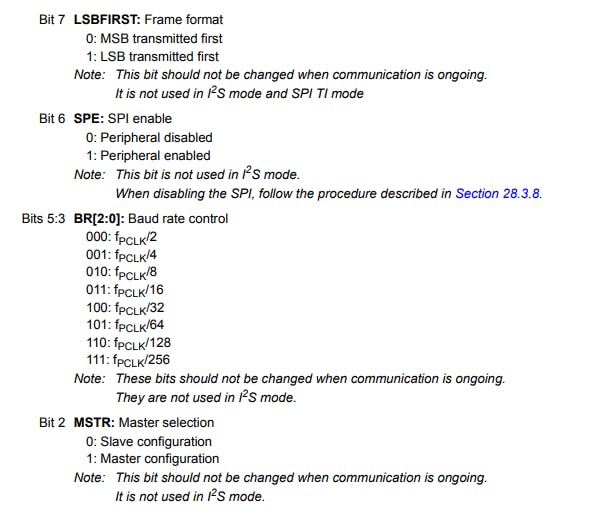
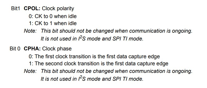
Then, the MSB-First mode is configured by writing a 0 to position 7 in the SPI1->CR1 register. After, that we set CPOL=0 and CPHA=0, as per the directions specified in the LIS302DL datasheet.
Finally, we enable SPI by writing a 1 to position 6 in the SPI1->CR1 register. CRC is enabled by writing a 1 to position 13 in the SPI1->CR1 register. Then, Motorola format is chosen by writing 0x0000 to the SPI1->CR2 register.
- Transmission is handled by the
uint16_t SPI_Transmit(uint8_t data)function,
uint16_t SPI_Transmit(uint8_t data){
    //  Wait until the TX buffer is empty, i.e. data is transmitted
    while(!((SPI1->SR) & SPI_SR_TXE)){}
    // Load the data into the data register
    SPI1->DR = data;

    while(!(SPI1->SR & SPI_SR_RXNE)){}
    // If reception is intended, read the value from the data register
    rxd = SPI1->DR;

    return rxd;
}
This function takes, in the data that needs to be transmitted as an argument of the type uint_8. Before queueing the data to be sent, we check if the Transmit buffer is empty, for that we poll the TXE bit in the SPI1->SR register. Then, we write the data to the SPI1->DR register.
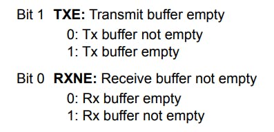
Once, the data is put into the transmit buffer, we poll the RXNE bit in the SPI1->DR register to determine if there is something in the receive buffer. Then, the SPI1->DR register is read to get the received message. This value is stored in the rxd variable, which is then returned at the end of the function.
- After, this let's look at the
uint16_t SPI_Receive(uint8_t addr)function, this is a wrapper function, which calls theSPI_Transmitfunction internally.
uint16_t SPI_Receive(uint8_t addr){
    GPIOE->BSRR |= GPIO_BSRR_BR3;
    addr |= 0x80;
    SPI_Transmit(addr);
    rxdf = SPI_Transmit(0);
    GPIOE->BSRR |= GPIO_BSRR_BS3;
    return rxdf;
}
In this function, the address(addr) of the register to be read is passed as an argument. We first select the accelerometer by pushing PE3 to 0 by writing a 1 to position 19 in the GPIOE->BSRR register. If you remember when we saw the timing diagram, I mentioned that when we need to receive data from the sensor, the first bit of the address needs to be 1, hence before sending the address, we perform the OR operation with itself and 0x80, which will set the MSB of the address. After that, we call the SPI_Transmit(addr) function, which takes in addr as a parameter. Here, we are not interested in the returned value so we do not bother about it. Then, we call the rxdf = SPI_Transmit(0) function, with rxdf getting the returned value and passing 0, i.e. a dummy value as an argument to the function. The shift register type mechanism writes a value of 0 to the slave register address, and the previous value is pushed out and communicated with the master, which is our development board. Finally, we deselect the sensor, by pushing PE3 to 1, in a similar manner as we pushed it to 0, by writing a 1 to position 3 in the GPIOE->BSRR register.
- Now, we look at the
void LIS_Write(uint8_t addr,uint8_t data)function,
void LIS_Write(uint8_t addr,uint8_t data){
    // Selecting the LIS accelerometer
    GPIOE->BSRR |= GPIO_BSRR_BR3;

    // Send the Register Address
    SPI_Transmit(addr);

    // Send the data to be written
    SPI_Transmit(data);

    // De-select the accelerometer
    GPIOE->BSRR |= GPIO_BSRR_BS3;
}
This is very similar to the uint16_t SPI_Receive(uint8_t addr) function, except here, we have two arguments addr and data. Also, the OR operation is not performed here, since we need to write to the slave register address.
- Then, comes the
void LIS_Init()function,
void LIS_Init(){
// Powering on the accelerometer and Enabling the x,y and z axis for acceleration capture
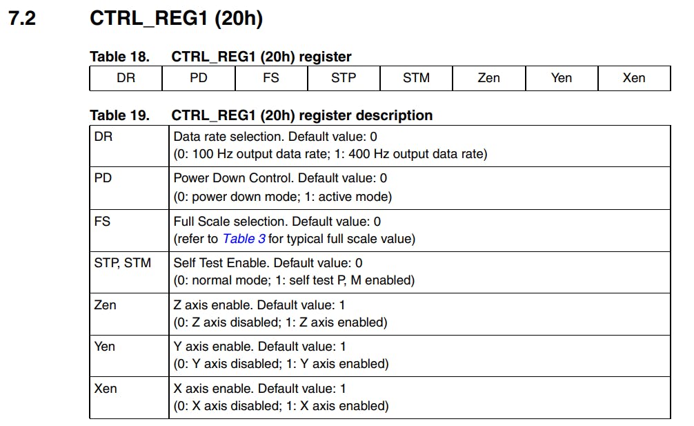
LIS_Write(CTRL_REG1, 0x47);
}
There isn't much done in this function, we just call LIS_Write(CTRL_REG1, 0x47) function, here to write a value of 0x47 to the CTRL_REG1 register on the LIS302DL sensor. The value 0x47 signifies that we are powering on the accelerometer, and enabling acceleration value capture for the x, y, and z axis.
- After that, there is the
void LIS_Read()function,
void LIS_Read(){
    // Reading the data for x-axis
    x = SPI_Receive(OUT_X);

    // Reading the data for y-axis
    y = SPI_Receive(OUT_Y);

    // Reading the data for z-axis
    z = SPI_Receive(OUT_Z);
}
This is a high-level read function, that reads the values from the x, y, and z data registers by calling the SPI_Receive function.
- The delay is provided by the void
TIM4_ms_Delay(uint32_t delay)function,
void TIM4_ms_Delay(uint16_t delay){
RCC->APB1ENR |= RCC_APB1ENR_TIM4EN; //Enable the clock for TIM3
TIM4->PSC = 16000-1; //Set the clock frequency to 1KHz
TIM4->ARR = delay; // Get the required delay from user
TIM4->CNT = 0;
TIM4->CR1 |= 1; // Start the timer
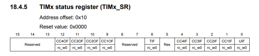
while(!(TIM4->SR & 1)){} // Wait for the "Update Interrupt Flag"
TIM4->SR &= ~(0x0001); // Clear the "Update Interrupt Flag"
}
Here, we enable the clock for the Timer 4, and set the Pre-scalar to 16000-1 to reduce the clock speed to 1 KHz, which means one clock tick corresponds to 1ms. After that, we assign the desired delay value to the TIM2->ARR register, initialize the count to zero and start the timer. Then we poll the UIF or the Update Interrupt Flag, which is set after the desired amount of clock ticks provided in the TIM2->ARR register are done, or in other words when the timer overflows. After the UIF flag is set we clear it from the TIM2->SR register and exit the function.
- The calibration is done by
int16_t Convert_To_Val(uint16_t val)function,
int16_t Convert_To_Val(uint16_t val){
    if ((val & 0x80) == 0x80){
        val = ~val;
        val += 1;
        val &= 0x00FF;
        val = ( val * 2300 ) / 127;
        return (-1 * val);
    }
    else
        return (( val * 2300 ) / 127);
}
The function accepts the value val as an argument, which is of type uint_16t. Here, we first check if the value obtained is negative, since the data written to the data registers in the sensor, is in 2's complement form. So, to do this, we perform the AND operation of val and 0x80, if the output is 0x80 then, we obtain the magnitude of the 2's complement number. After that, we make sure only the last 8-bits are obtained as outputs since, the output data registers on the accelerometer are 8-bits wide. Then, we multiply the magnitude with 2300, since the default acceleration data is \(\pm 2.3g\) , and a factor of 1000 is there for convenience. Then, the value is divided by 127 since the data is 8-bits. Finally based on the sign the value is returned.
6. Writing the main function
int main(void){
    GPIO_Init();
    SPI_Init();
    LIS_Init();
    GPIOE->BSRR |= GPIO_BSRR_BS3;
    while(1){
        // Call the read function
        LIS_Read();

        // Use the Convert_To_Val function to convert raw data into actual data
        x_final = Convert_To_Val(x) + X_OFFSET;
        y_final = Convert_To_Val(y);

        // Switch on LEDs based on the acceleration value obtained
        if ((x_final != 0) && (y_final != 0)){
            if (x_final > THRESH_HIGH){
                GPIOD->ODR |= GPIO_ODR_OD14;
                GPIOD->ODR &= ~(GPIO_ODR_OD12 | GPIO_ODR_OD13 | GPIO_ODR_OD15);
            }
            else if (x_final < THRESH_LOW){
                GPIOD->ODR |= GPIO_ODR_OD12;
                GPIOD->ODR &= ~(GPIO_ODR_OD14 | GPIO_ODR_OD13 | GPIO_ODR_OD15);
            }
            if (y_final > THRESH_HIGH){
                GPIOD->ODR |= GPIO_ODR_OD13;
                GPIOD->ODR &= ~(GPIO_ODR_OD12 | GPIO_ODR_OD14 | GPIO_ODR_OD15);
            }
            else if (y_final < THRESH_LOW ){
                GPIOD->ODR |= GPIO_ODR_OD15;
                GPIOD->ODR &= ~(GPIO_ODR_OD12 | GPIO_ODR_OD13 | GPIO_ODR_OD14);
            }
        }
        else
            GPIOD->ODR &= ~(GPIO_ODR_OD12 | GPIO_ODR_OD13 | GPIO_ODR_OD14 | GPIO_ODR_OD15);

        // Give a finite delay
        TIM4_ms_Delay(20);
    }
}
In the beginning of the main function, we initialize all of our peripherals and devices, by calling GPIO_Init(), SPI_Init(), and LIS_Init() functions. As we just saw, these functions will configure our GPIO pins, SPI1, as well as the LIS302DL sensor. After that we initiate communication with the accelerometer by pushing PE3 to 0. This is done by writing a 1 to position 3, in the GPIOE->BSRR register. Then, we start an infinite loop, in which we first call the LIS_READ() function, to read the acceleration values, for x, y, and z direction. Then, we calculate the processed value for the x and y direction, by adding any offset if required to the value obtained from the Convert_To_Val function. This offset is determined by adjusting any discrepancy in the resting value of the accelerometer.
After that, we move on to the logic for toggling the LEDs. Now, when the acceleration values are at 0, we do not want to light up any LEDs, so we first check if we have non-zero acceleration values for the x and y axis. If indeed, we have non-zero acceleration values, then we check the values based on the thresholds that were defined at the beginning of the file. These values are decided by testing, you are free to play with them yourself and see the difference. The LEDs are toggled based on their physical arrangement on the board, and when one of them, if switched on, the others are toggled off. Also, if we have acceleration values to be 0, all of the LEDs, are switched off. Finally, in the end, we give a delay of 20ms, to enable smooth functioning of the application.
That marks the end of our code. Let's move on to the results now.
Conclusion
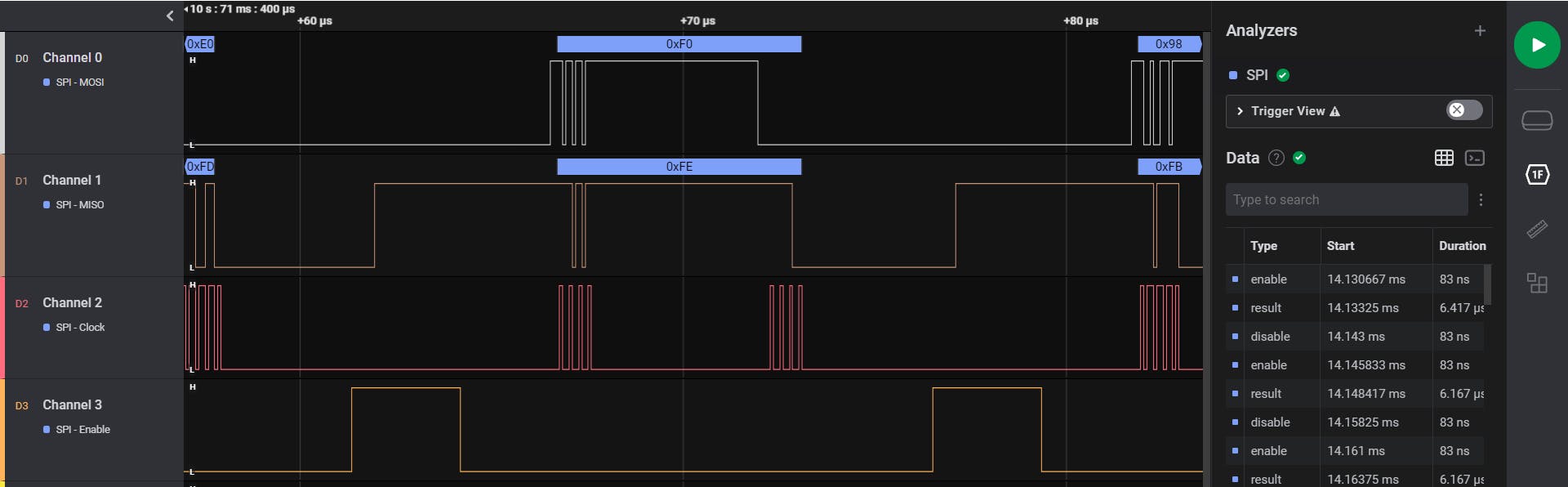
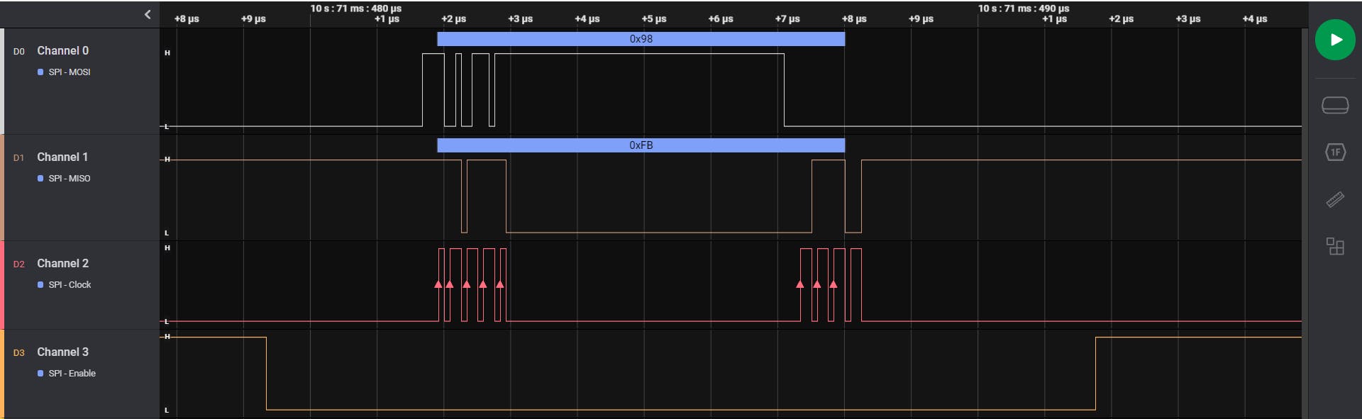
In this section, we will look at some screenshots from the Logic Analyzer, and then move on to the demo. In the figures below, you can see the CS pin is pushed to low for communication, the master sends out data, and immediately, we see the previous value from the slave register, communicated via MISO. The clock also operates based on the CPOL and CPHA parameters, that we configured.
I hope you found this article useful and easy to follow. All the code used here will be available in my GitHub repo, which can be accessed by clicking here, and the demo for this tutorial can be found by clicking here.