Servo Motor Control with a Potentiometer using the STM32F407 Discovery Kit


Introduction
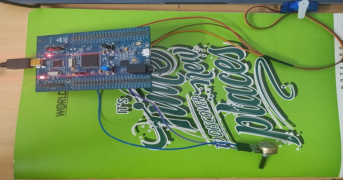
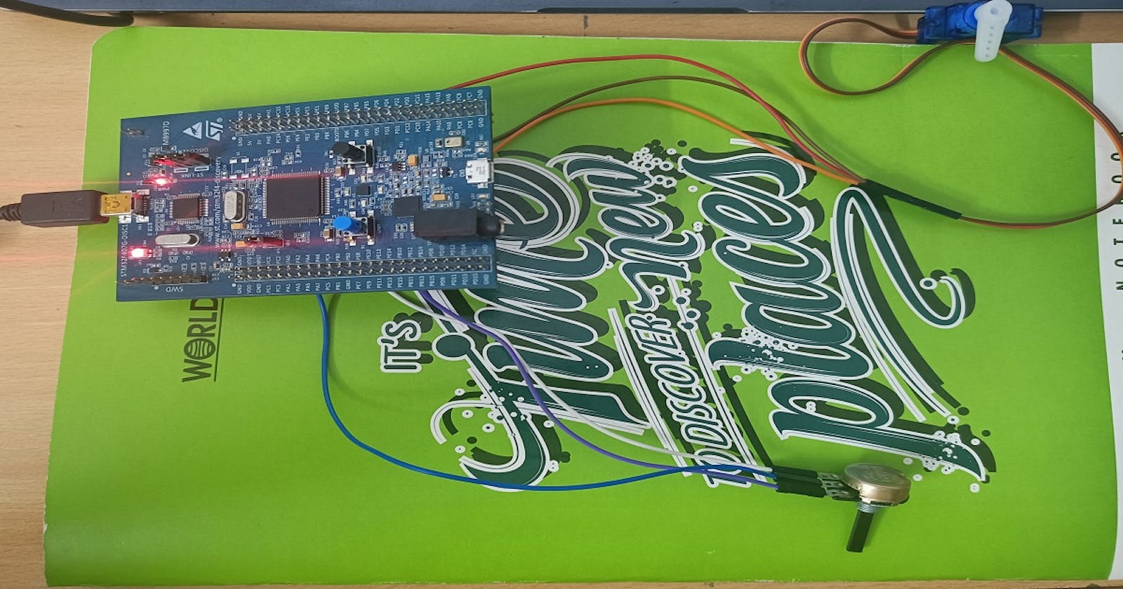
Hi! 😄Today our aim will be to use the ADC peripheral available on the STM32F407 Discovery Kit. It is used to convert the analog value given out by a sensor to digital values into a specific resolution (12-bit, 8-bit, 10-bit, etc.) configured by the programmer. We will continue our tradition and use Bare Metal Programming to achieve this task as well. A potentiometer will act as our source of analog values to be converted, whose output will be connected to a GPIO pin on our development kit, through which we will process the data. But, we will not just be using an ADC in this project, a servo motor (sg90) will also be used to show how the output from the ADC can be mapped to other devices and how those values can be used to control them.
Working Principle
ADC and Potentiometer
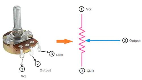
The potentiometer is basically a variable resistor. It has a total of 3 Terminals, where the outermost terminals need to be connected to VCC and GND, and the terminal in the middle will give us our analog output. It consists of a knob that is turned to control the resistance value of the potentiometer, this value of resistance will, in turn, affect the voltage drop across it, and that voltage will act as our analog value which needs to be converted into a digital form.
Now let's talk about the ADC. The STM32F407 Discovery Kit consists of 3 ADCs, each of these has 16 Independent Channels which can convert various analog inputs into their corresponding digital values. All of these ADC are successive approximation type and can be configured in 12-bit, 10-bit, 8-bit, and 6-bit resolution modes. The conversion takes place based on the following formula,
$$ D = (V_{Ref})/((2^n) -1) $$
Where,
n - The resolution of the ADC
\(V_{Ref}\) - The reference voltage for the ADC
D - The Digital Level or Value
The Digital Value obtained above lies in a specific range that depends on the resolution of the ADC. For example, in our case, we will be using ADC1 in 12-bit resolution mode, so the Digital Result will lie in the range of 0 to 4095 which is determined by \(2^n - 1\).
Another important factor of the ADC is its sampling rate. The sampling frequency always needs to be greater than twice the message frequency to accurately capture and convert the analog signal, according to the Nyquist Criteria. This factor determines how many samples are taken per second, which in turn will affect both the speed and accuracy of the conversion.
Servo Motor
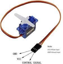
Here, I will be using the sg90 servo motor, which has a 180 degree range of motion. We can control the position of this motor by sending the PWM pulses to the control signal pin, which is shown in the figure above. The VCC and GND are connected to the 5V and GND of the microcontroller respectively. For detailed connections, please visit my GitHub repo, by clicking here.
As seen in the figure below, the time period of the pulse to be generated needs to be 20ms, or in other words, it must have a frequency of 50 Hz. Out of that period, the T on (The time duration for which the state must be HIGH) should be 1ms for moving the motor to the 0 degree position and 2ms for moving the motor to the 180 degrees position.
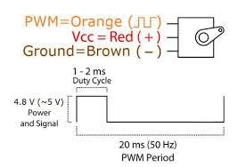
Note: While testing the motor, I could not achieve the full range of its motion by sending pulses with pulse widths between 1ms and 2ms. So, by trial and error, I figured out the actual range of motion can be achieved by sending pulses with pulse-widths between 0.5ms and 2.5ms for the 0 degree and 180 degrees position respectively. This is what I have used in my code as well, as you will see in the latter part of this blog.
Components Required
STM32F4 based microcontroller
An sg90 servo motor
A potentiometer
A few Jumper wires
After gathering all the aforementioned components we are ready to start programming our microcontroller 😀.
Programming the MCU
I have used bare-metal programming for the coding, which involves Bitwise AND/OR/XOR operations on the SFRs (Special Function Registers) present on the MCU.
1. Including the necessary Header Files
#include "stm32f4xx.h"
#define ARM_MATH_CM4
These are the header files included at the top of our main.c file. The stm32f4xx.h is the one for our microcontroller and the ARM_MATH_CM4 is for any math operations that we perform in our code.
2. Declaring the User-Defined Functions and Variables
void GPIO_Init(void);
void ADC1_Init(void);
void TIM2_Init(void);
void TIM4_ms_Delay(uint32_t delay);
int u;
The GPIO_Init(void) function is used to configure all the GPIO pins that we will require to use the ADC and control our servo motor, which will be PC0 and PA5 respectively. Then in the ADC1_Init(void) function, we configure the various parameters of the ADC and initialize it. After that, the TIM2_Init(void) function is used to generate the PWM pulses that will be used for the servo motor control. Lastly, the TIM4_ms_Delay(uint32_t delay) is used to provide a delay in milliseconds as the name suggests, for the actuation of the servo motor after it has been instructed to move. The int u variable will store the digital values given out by our ADC1 which will be mapped to the pulse width of the PWM signal that has to be used to control the servo motor.
3. Defining the User-Defined Functions
- First, let's take a look at
GPIO_Init(),
void GPIO_Init(){
//PC0 is connected to ADC1 IN10
RCC->AHB1ENR |= RCC_AHB1ENR_GPIOCEN;// Enable GPIOC clock
GPIOC->MODER |= GPIO_MODER_MODER0; // Set PC0 to Analog mode
RCC->AHB1ENR |= 1; //Enable GPIOA clock
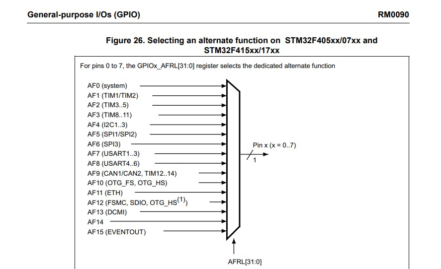
GPIOA->AFR[0] |= 0x00100000; // Select the PA5 pin in alternate function mode
GPIOA->MODER |= 0x00000800; //Set the PA5 pin alternate function
}
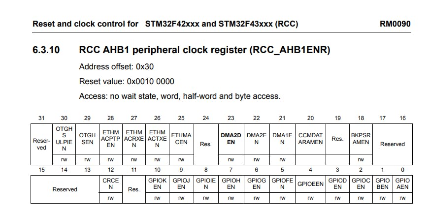
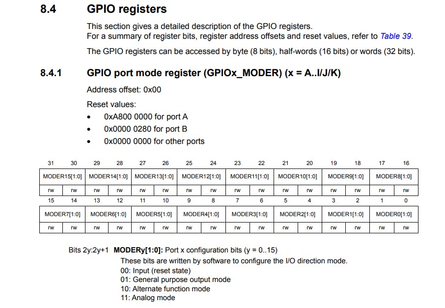
Here, we first enable the clock signal for GPIO Port C by setting the GPIOCEN bit to 1 in the RCC->AHB1ENR register. Then we set PC0 to Analog mode by writing 11 to the MODER0[1:0] bits in the GPIOC->MODER register. We are going to use PC0 for our analog input pin since it is connected to ADC1 IN10 that is channel 10 of ADC1 on our MCU.
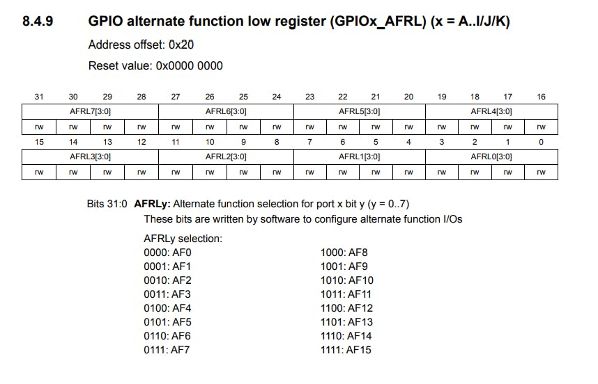
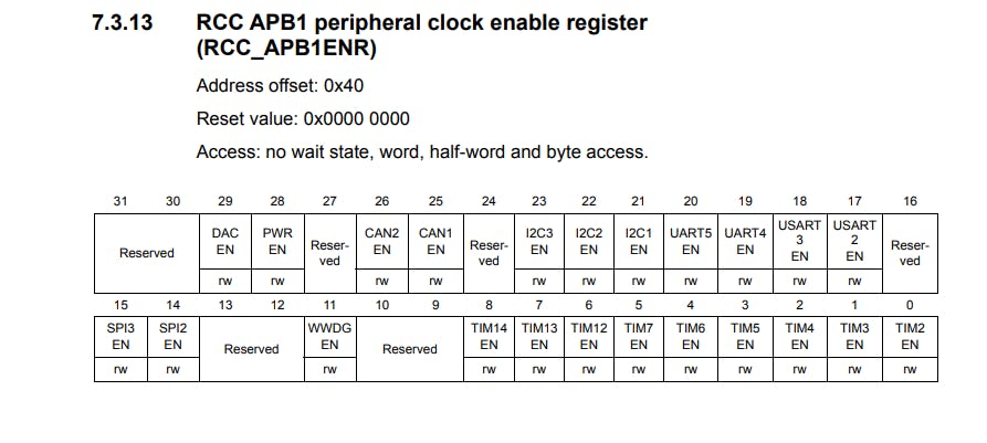
Then, for our PWM generation, we configure PA5 in Alternate Function Mode, because one of its alternate functions is Channel 1 of Timer 2. So, we enable the clock signal for GPIO Port A by setting the GPIOAEN bit to 1 in the RCC->AHB1ENR register. After that, we set PA5 in alternate function mode by writing 10 to the MODER5[1:0] bits in the GPIOA->MODER register. Then we write 0001 to AFRL5[3:0] bits in the GPIOA->AFR[0] register. The pictures describing these registers are given above.
- Now, comes the
ADC1_Init()function,
void ADC1_Init(){
RCC->APB2ENR |= RCC_APB2ENR_ADC1EN;//Enable ADC clock
//APB2 clock is not divided so it runs at 16MHz
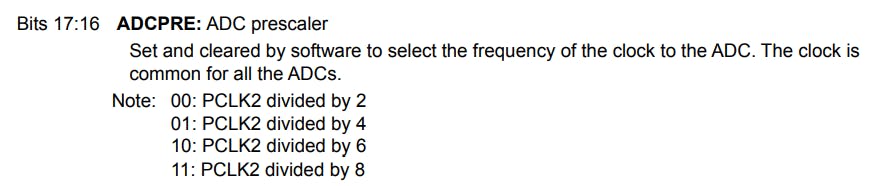
ADC->CCR |= 0<<16; // PCLK2 divide by 2, so the clock frequency is 8MHz
ADC1->CR2 |= ADC_CR2_CONT; // Setting the Continuous Conversion Mode
ADC1->CR2 |= ADC_CR2_ADON; // Enabling the ADC
ADC1->CR2 &= ~ADC_CR2_ALIGN; //setting the alignment to the right
ADC1->CR1 &= ~ADC_CR1_RES; // Selecting 12-bit resolution
ADC1->SMPR1 |= (ADC_SMPR2_SMP0_0 | ADC_SMPR2_SMP0_2); // 112 Sampling cycle selection
ADC1->SQR3 |= 10<<0; // Selecting channel 10
}
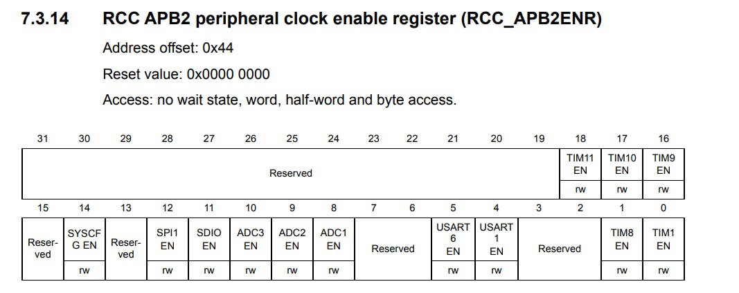
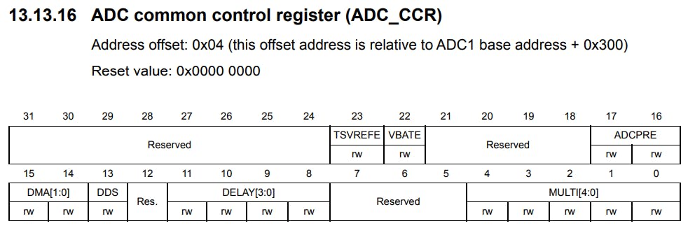
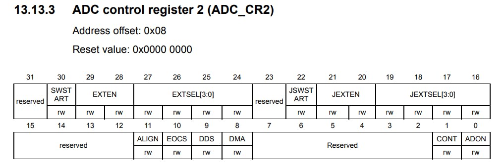
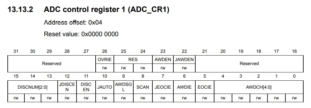
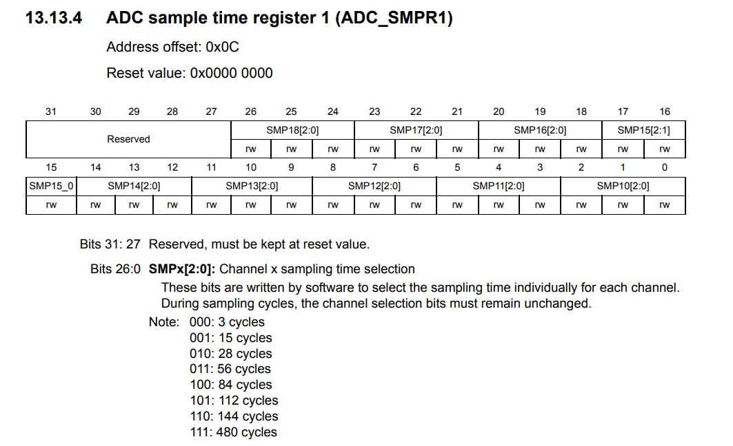
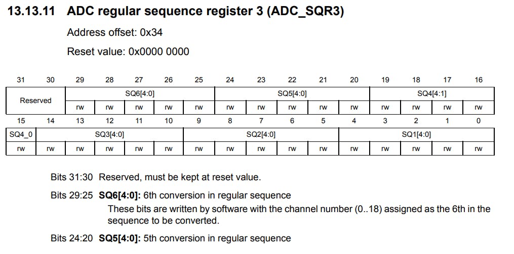
Here, we first enable the clock for ADC1 by writing a 1 to the ADC1EN bit in the RCC->APB2ENR register, and since we don't divide the APB2 clock it will work at 16MHz. Then we start configuring the ADC. For that, first, we divide the PCLK2 by 2 so that, the ADC1 will run at 8MHz. This is done by writing a 0 to the ADCPRE bits in the ADC->CCR register, which signifies clock division by 2. Then we set the Continuous Conversion Mode for ADC1 by writing a 1 to the CONT bit in the ADC1->CR2 register. After that, we Enable the ADC and align our data to the right by writing a 1 to the ADON bit and a 0 to the ALIGN bit in the ADC1->CR2 register respectively. For selecting our ADC resolution we write a 00 to the RES[1:0] bits in the ADC1->CR1 register, which signifies the 12-bit resolution mode. Next, we need to configure the sampling rate for our ADC which is done by writing 101 to the SMP10[2:0] bits in the ADC1->SMPR1 register which signifies a sampling rate of 112 cycles. Then, in the end, we set the ADC channel conversion sequence by setting it as first in the regular sequence. This is done by writing 10 (since our channel number is 10) to the SQ1[4:0] bits in the ADC1->SQR3 register.
- Now, let's look at
void TIM2_Init(),
void TIM2_Init(){
RCC->APB1ENR |=1;
TIM2->PSC = 16-1; //Setting the clock frequency to 1MHz.
TIM2->ARR = 20000; // Total period of the timer
TIM2->CNT = 0;
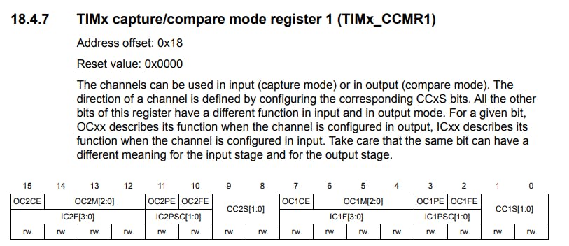
TIM2->CCMR1 = 0x0060; //PWM mode for the timer
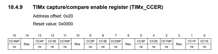
TIM2->CCER |= 1; //Enable channel 1 as output
TIM2->CCR1 = 500; // Pulse width for PWM
}
Here, we start by enabling the clock for the Timer 2, because we will be using it to generate our pulses. This is done by writing a 1 to the TIM2EN bit of the RCC->APB1ENR register. Then, we set the Pre-scalar to 16-1 to reduce the clock frequency to 1MHz from 16MHz, by writing the value to the TIM2->PSC register. After that, we set the time period of the pulse to be generated by assigning the corresponding value to the TIM2->ARR register, which is 20,000 in this case since we want the time period to be 20ms. Each timer tick corresponds to (1 / (1 MHz)), which is 1 micro-second, and since we require the time period to be 20ms the TIM2->ARR register is loaded with 20x1000 micro-seconds, which is 20 milliseconds. Then, we initialize the TIM2-CNT to zero.
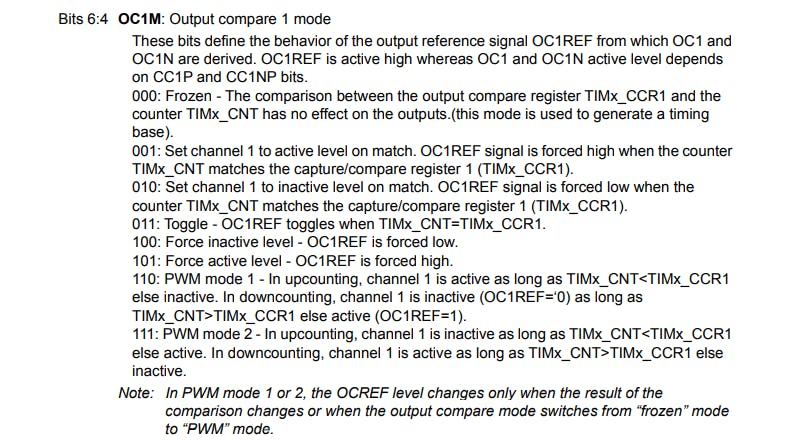
After that, we configure PWM Mode 1 for TImer 2 - Channel 1, and make Channel 1 an output. For that, we first write 0110 to the OC1M bits of the TIM2->CCMR1 register.
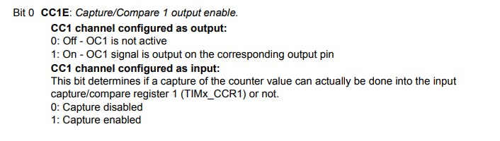
Then, we enable the PWM output on Channel 1 by writing a 1 to the CC1E bit in the TIM2->CCER register.
Finally, we set the initial Pulse-Width or initial Angle for the motor, by setting the TIM2->CCR1 register. Here, I have chosen the 0 degrees position as the initial position for my servo motor, by assigning a value of 500 or 0.5ms to the TIM2->CCR1 register.
- Then, comes the
void TIM4_ms_Delay(uint32_t delay)function, which handles any time delay requirements that are needed, in themainfunction.
void TIM4_ms_Delay(uint32_t delay){
RCC->APB1ENR |= 1<<2; //Start the clock for the timer peripheral
TIM4->PSC = 16000-1; //Setting the clock frequency to 1kHz.
TIM4->ARR = (delay); // Total period of the timer
TIM4->CNT = 0;
TIM4->CR1 |= 1; //Start the Timer
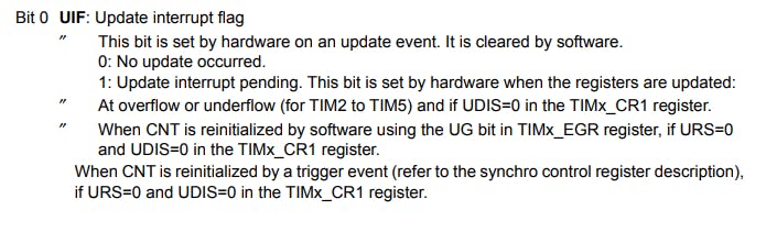
while(!(TIM4->SR & TIM_SR_UIF)){} //Polling the update interrupt flag
TIM4->SR &= ~(0x0001); //Reset the update interrupt flag
}
Most of the configurations done here are very similar to the ones I described above for the function void TIM2_Init(). Here, we enable the clock for the Timer 4, and set the Pre-scalar to 16000-1 to reduce the clock speed to 1 KHz, which means one clock tick corresponds to 1ms. After that, we assign the desired delay value to the TIM2->ARR register, initialize the count to zero and start the timer. Then we poll the UIF or the Update Interrupt Flag, which is set after the desired amount of clock ticks provided in the TIM2->ARR register are done, or in other words when the timer overflows. After the UIF flag is set we clear it from the TIM2->SR register and exit the function.
4. Writing the main Function
int main(void){
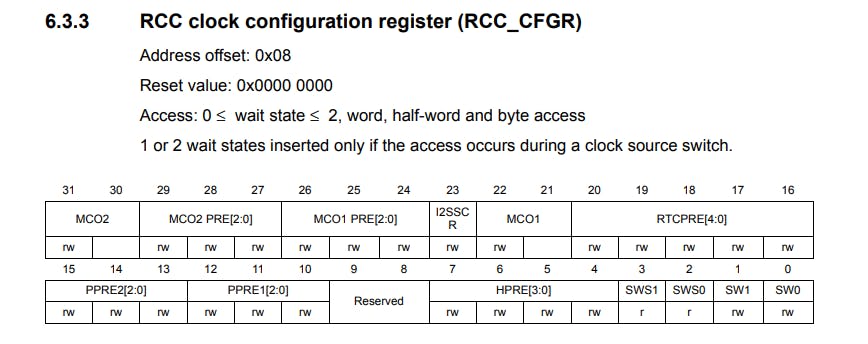
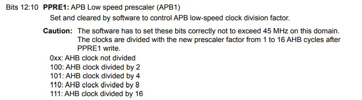
RCC->CFGR |= 0<<10; // set APB1 = 16 MHz
GPIO_Init();
ADC1_Init();
TIM2_Init();
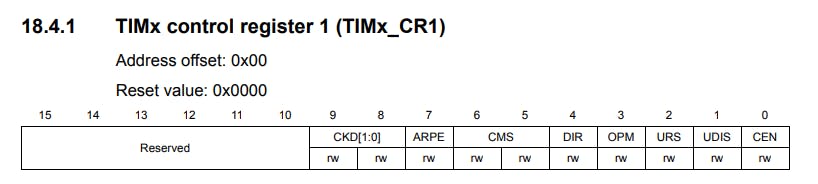
TIM2->CR1 |= 1;
while(1){
ADC1->CR2 |= ADC_CR2_SWSTART; //Starting ADC conversion
while (!(ADC1->SR & ADC_SR_EOC)){}
u = ADC1->DR;
TIM2->CCR1 = (int)(((u/4095)*2000)+500);
TIM4_ms_Delay(50);
}
}
Here, we first set the APB1 clock speed to 16 MHz, by writing a zero to the PPRE[3:0] bits in the RCC->CFGR register, and then we call all the initialization functions we defined above.
Then, we start the Timer 2 by writing a 1 to the CEN bit in the TIM2->CR1 register. By, doing this we start getting the PWM pulses with a pulse width of 0.5ms on PA5.
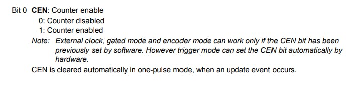
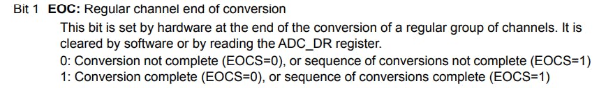
After that, we enter the infinite while loop, here we start the ADC conversion by writing a 1 to the SWSTART bit in the ADC1->CR2 register. After that, we poll the EOC flag in the ADC1->SR register, since it signifies the End of Conversion. Then we read the converted value from the ADC1->DR register and store it in the variable u which we had defined earlier.
Our next step is to map the value we obtained from the pot to the range of pulse width required to control the servo motor. To do that we use the following line,
TIM2->CCR1 = (int)(((u/4095)*2000)+500);. In this, first, we are converting our input to a range of 0 to 1 by dividing u by 4095 (Since it's a 12-bit ADC). Then, we multiply the value by 2000 since the servo motor has a control range of 500 to 2500, the latter representing the 180 degrees position and the former representing the 0 degrees position respectively. So, when we subtract 2500 from 500 we get 2000. After that, we add 500 to the resulting value to ensure that the servo motor receives a pulse-width value that is within its control range. This calculated value is finally given to TIM2->CCR1 register by converting it into the corresponding int value. A delay of 50ms is given for the motor to acknowledge the change in the pulse-width and move to the desired position.
We keep repeating this process indefinitely, and hence we are able to achieve control over the movement of a servo motor.
Conclusion
With that, we have been able to successfully control the sg90 servo motor by turning the knob of a potentiometer😄.
I hope you found this article useful and easy to follow along😀. All the codes used here are present in my GitHub repository, which you can access by clicking here.
And, the demo video for this tutorial can be found here.