Testing the CAN peripheral on the STM32F407 Discovery Kit in Loopback Mode


Introduction
Hello!! 😄 Today we will explore the CAN peripheral available on the STM32F407 Discovery Kit. We will test it using the Loopback Operating mode, which is one of the Test modes. The purpose of this test is to ensure that the CAN peripheral is working properly, and in our case also acts as a starting point in the journey to learn about the CAN Communication Protocol. The main idea of the Loopback test is that there is only one node on the CAN bus, and that same node receives the data that it transmits. As the name suggests the data that is transmitted by the node loops back towards it.
Working Principle
CAN Protocol
CAN stands for Controller Area Network. It was first created by the German Automotive Company Robert Bosch in the mid-1980s for automobile applications.
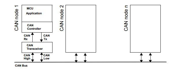
CAN is a message-based protocol, which means that communication does not happen based on addresses but rather the CAN message itself contains the priority and the data that needs to be transmitted. Every node on the bus receives this message, and then each node decides whether that information is useful or needs to be discarded. A single message can be destined for a particular receiver or for multiple nodes that are present on the bus.
Another important feature of the CAN protocol is its ability to request information from other nodes which is known as Remote Transmission Request or RTR. Since CAN is a message-based protocol a node can be added to the system without the need to reprogram the other nodes for acknowledging the new addition.
A CAN data frame can be represented as:
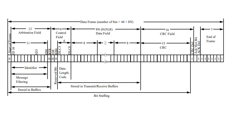
The elements of a CAN Frame are:
SOF – Start of Frame
Identifier – A message Identifier that sets the priority of the Data Frame.
RTR – Remote Transmission Request, defines the frame type (data frame or remote frame – 1 Bit)
Control Field – User-Defined Functions
DLC – Data Length Code (4 bits)
Data Field – User-Defined Data (0 to 8 Bytes)
CRC Filed – Cyclic Redundancy checks for Error (Data corruption) detection.
ACK Field - Receivers Acknowledgement
CAN network topology,
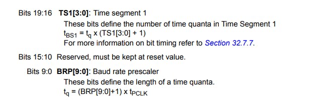
The CAN Loopback mode can be understood by the following figure,
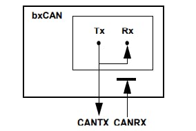
As can be seen in the above figure, the node that is transmitting the data is the same as the one receiving it. The data that the node transmits comes back at it and is received by it, which emulates the behavior of a normal node on the CAN Bus.
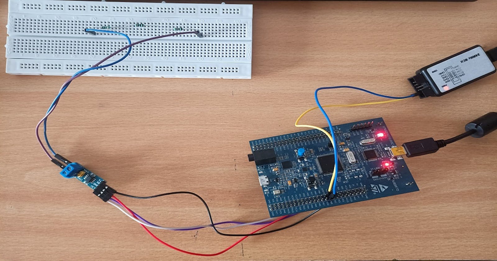
For implementing the CAN protocol on our MCU, we will need a CAN transceiver. The STM32F407 microcontroller has an in-built CAN controller, but the CAN transceiver needs to be connected externally. So, we will be using the SN65HVD230 for that purpose. Now, the CAN Bus needs to be terminated by connecting a 120-ohm resistance between CAN High and CAN Low. These are basically the two wires that make up the CAN Bus, which acts as a medium for communication between the various nodes. If the CAN Bus is not terminated by a resistance the transmitted messages might reflect back and corrupt the messages on the bus and lead to a communication failure. The SN65HVD230 breakout board does not come with a 120-ohm on-board termination, so we will need to connect it externally.
Now let's talk about how the reception is handled at each node. Since CAN is a message-based protocol, each node is identified by the Identifier Field that is embedded in the CAN Frame. So, each node on the CAN bus can be configured to receive messages either from only a specific node or a particular group of nodes based on the identifier of the incoming message. This is achieved by using the filters that are available in the CAN controllers. The filters are a part of the hardware so the unwanted messages are discarded before they even reach the CPU of the microcontroller, this helps save time as well as resources that can be used elsewhere for more important tasks, and this is especially helpful since the number of resources in an embedded system is constrained. The filters can be configured in Indentifer List Mode or Mask Mode. In the Mask Mode the filters are configured to match some of the bits at a specific position in the identifier of the transmitted message if they match only then the message is accepted by that particular node, otherwise, it is discarded. This mode can be used when a particular node wants to receive messages from a specific group of nodes. While, in the Identifier List Mode, all the bits in the Identifier Field of the incoming message must match the pre-configured value in the filter register for the node to accept that message. This mode can be used when a node wants to receive messages only from a particular node on the CAN Bus.
The Connections that need to be made, can be found in my GitHub repo, which you can access by clicking here.
Enough theory, now let's start the interesting stuff!! 😀
Components Required
An STM32F4 based MCU
A SN65HVD230 Breakout board
A 120-ohm resistor OR any combination of registers that results in 120-ohms ( I have used two 10-ohm resistors and a 100-ohm resistor and connected them in series to get 120-ohms).
A Logic Analyzer
A Few Jumper Wires
A breadboard
And, that's all. After gathering these components we are ready to start coding.
Programming our MCU
1. Including the necessary Header Files and some comments about the code
/******************************************************************************
 * Configurations are made as follows:
 * PB8 - CAN1_RX (Need to be set in AF9 for CAN1/CAN2)
 * PB9 - CAN1_TX (Need to be set in AF9 for CAN1/CAN2)
 *
 * The following is a bare metal code written for CAN Loop back test on the
 * Arm Cortex-M4 based STM32F407 Discovery Kit.
 *
 * @File   main.c
 * @Author Ruturaj A. Nanoti
 *****************************************************************************/

#include "stm32f4xx.h"
#define ARM_MATH_CM4
These are the header files included at the top of our main.c file. The stm32f4xx.h is the one for our microcontroller and the ARM_MATH_CM4 is for any math operations that we perform in our code.
2. Declaring the User-Defined Functions and variables
void GPIO_Init(void);
void CAN1_Init(void);
void CAN1_Tx(uint8_t tr);
uint8_t CAN1_Rx(void);
void TIM4_ms_Delay(uint32_t delay);
uint8_t k = 0;
uint8_t rec = 0;
The void GPIO_Init(void) function is used to initialize and configure the GPIO pins that we will be needing to connect our SN65HVD230 module and use the CAN Peripheral. The void CAN1_Init(void) and the void CAN1_Tx(uint8_t tr) functions are used to initialize CAN1 and transmit a byte of data respectively. The uint8_t CAN1_Rx(void) function is used to receive the incoming data. void TIM4_ms_Delay(uint32_t delay) acts as our delay function which utilizes the TIM4 peripheral and provides a delay in milliseconds. Finally, we declare the variables uint8_t k and uint8_t rec which will use to transmit and receive data respectively.
3. Defining the User-Defined Functions
- Let's configure the GPIO pins using the
void GPIO_Init()function,
void GPIO_Init(){
// Enable GPIOA clock signal
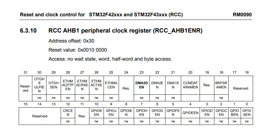
RCC->AHB1ENR |= RCC_AHB1ENR_GPIOBEN;
// Configuring PB8 and PB9 in alternate function mode
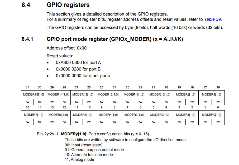
GPIOB->MODER |= (GPIO_MODER_MODER8_1 | GPIO_MODER_MODER9_1);
// Selecting AF9 for PB8 and PB9 (See Page 272 of dm00031020)
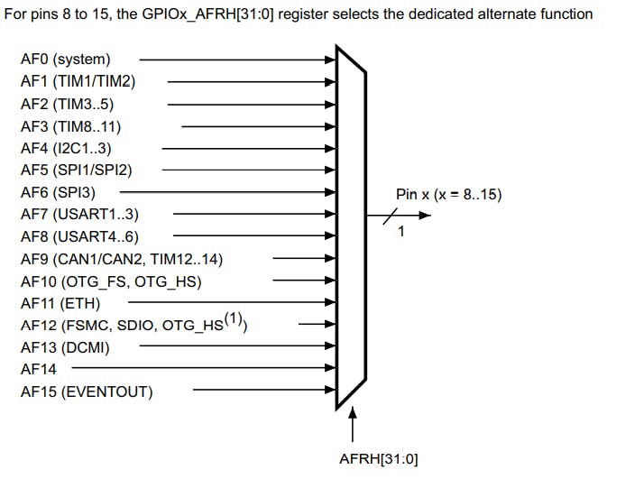
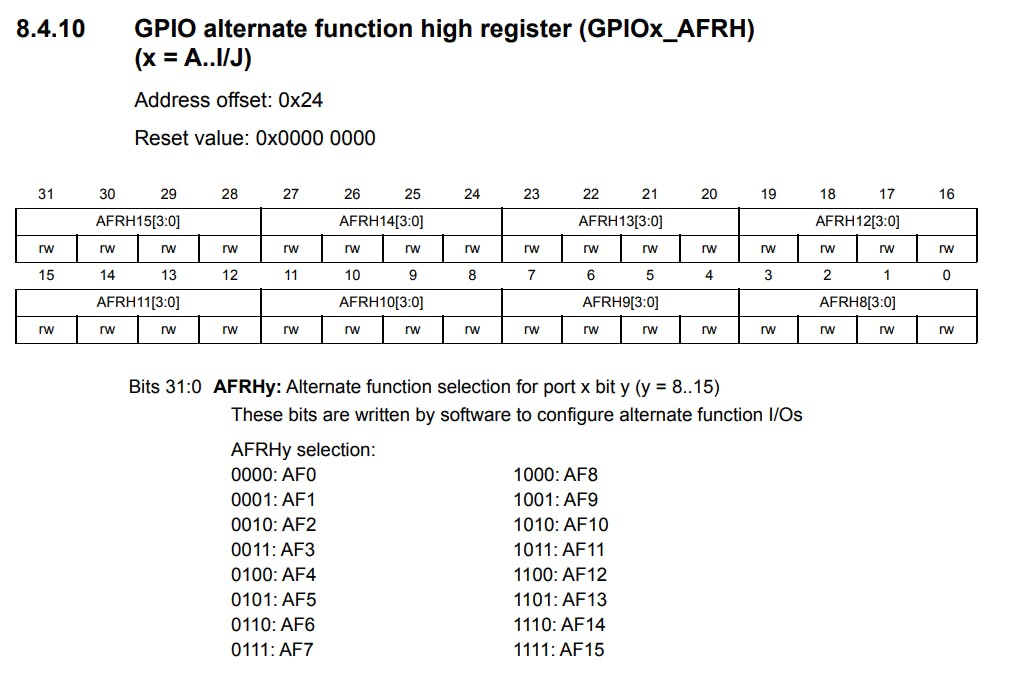
GPIOB->AFR[1] |= (GPIO_AFRH_AFSEL8_3 | GPIO_AFRH_AFSEL8_0 |
GPIO_AFRH_AFSEL9_0 | GPIO_AFRH_AFSEL9_3);
}
First, we enable the GPIOA clock by writing a 1 to the GPIOBEN bit in the RCC->AHB1ENR register.
Then, we set PB8 and PB9 in Alternate-Function Mode. This is done by writing 10 to the MODER8[1:0] and MODER9[1:0] bits in the GPIOB->MODER register.
We need to select AF9 for the CAN1 peripheral. This is done by writing 1001 to the AFRH8[3:0] and the AFRH9[3:0] bits in the GPIOB->AFR[1] register.
- Then, we come to our
void CAN1_Init()where we initialize and configure theCAN1peripheral,
void CAN1_Init(){
/* 1. Setting Up the Baud Rate and Configuring CAN1 in
* Loop Back Mode -------------------------------------------------------*/
// Enable clock for CAN1
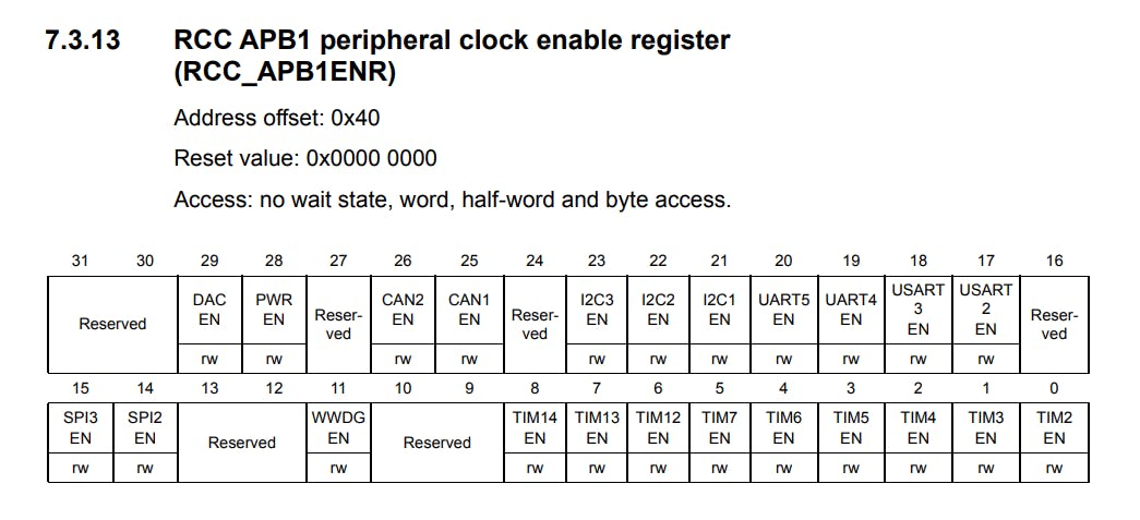
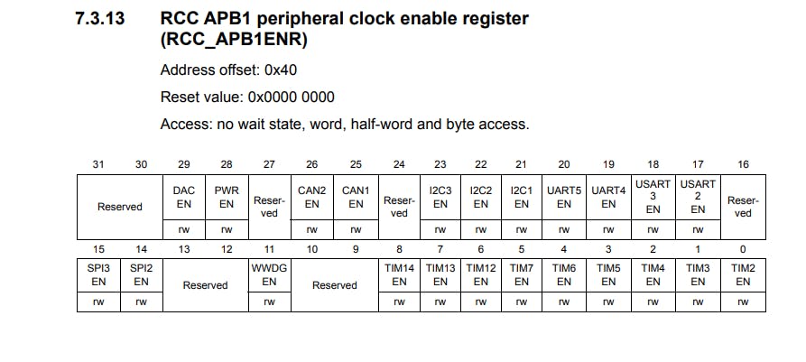
RCC->APB1ENR |= RCC_APB1ENR_CAN1EN;
// Entering CAN Initialization Mode and wait for acknowledgment
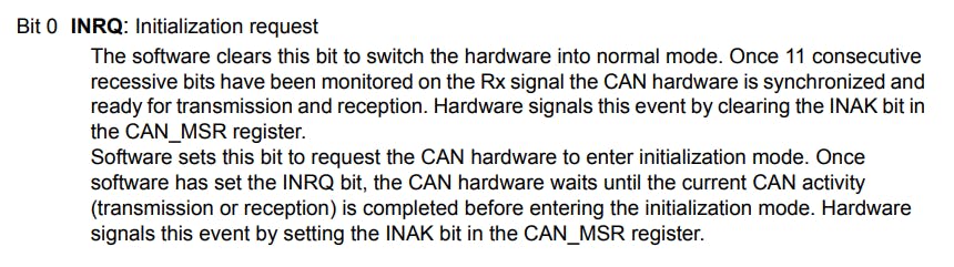
CAN1->MCR |= CAN_MCR_INRQ;
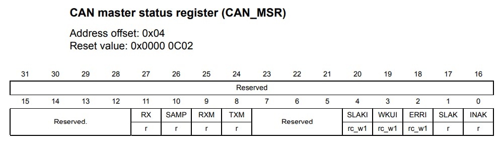
while (!(CAN1->MSR & CAN_MSR_INAK)){}
//Set Loop back mode for CAN1
CAN1->BTR |= CAN_BTR_LBKM;
//Setting the Re synchronization jump width to 1
CAN1->BTR &= ~CAN_BTR_SJW;
//Setting the no. of time quanta for Time segment 2
// TS2 = 4-1;
CAN1->BTR &= ~(CAN_BTR_TS2);
CAN1->BTR |= (CAN_BTR_TS2_1 | CAN_BTR_TS2_0);
//Setting the no. of time quanta for Time segment 1
// TS1 = 3-1;
CAN1->BTR &= ~(CAN_BTR_TS1);
CAN1->BTR |= (CAN_BTR_TS1_1);
//Setting the Baud rate Pre-scalar for CAN1
// BRP[9:0] = 16-1
CAN1->BTR |= ((16-1)<<0);
// Exit the Initialization mode for CAN1
// Wait until the INAK bit is cleared by hardware
CAN1->MCR &= ~CAN_MCR_INRQ;
while (CAN1->MSR & CAN_MSR_INAK){}
//Exit Sleep Mode
CAN1->MCR &= ~ CAN_MCR_SLEEP;
while (CAN1->MSR & CAN_MSR_SLAK){}
/* 2. Setting up the Transmission----------------------------------------*/
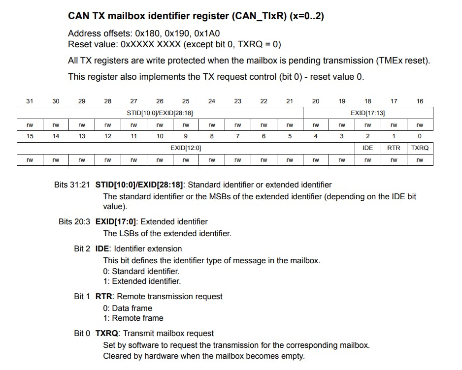
CAN1->sTxMailBox[0].TIR = 0;
//Setting up the Std. ID
CAN1->sTxMailBox[0].TIR = (0x245<<21);
CAN1->sTxMailBox[0].TDHR = 0;
// Setting Data Length to 1 Byte.
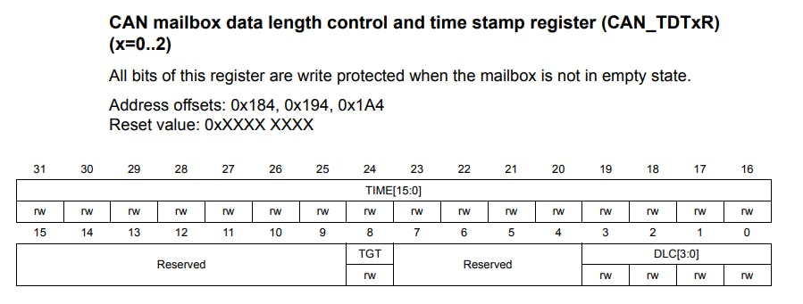
CAN1->sTxMailBox[0].TDTR = 1;
/* 3. Configuring the Filters--------------------------------------------*/
//Enter Filter Initialization mode to configure the filters
CAN1->FMR |= CAN_FMR_FINIT;
// Configuring the Number of Filters Reserved for CAN1
// and also the start bank for CAN2
CAN1->FMR |= 14<<8;
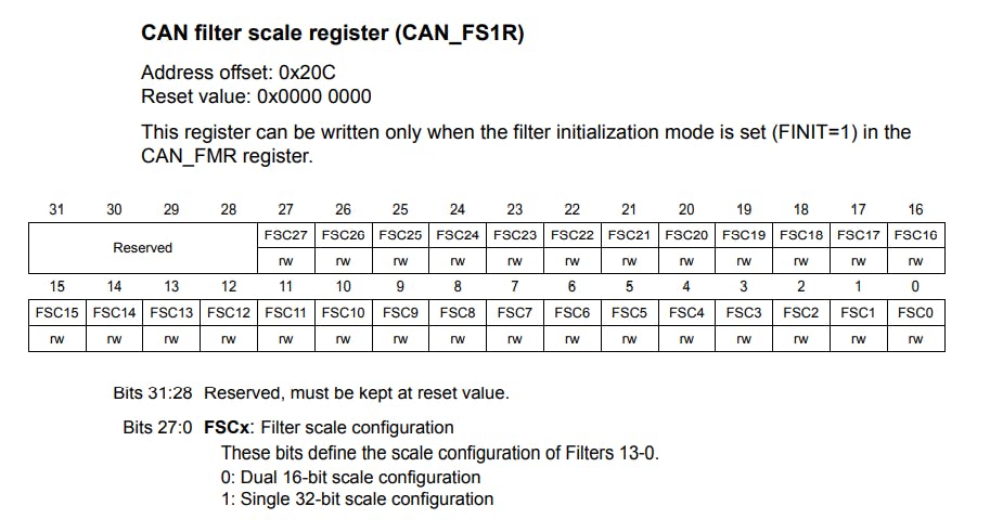
// Select the single 32-bit scale configuration
CAN1->FS1R |= CAN_FS1R_FSC13;
// Set the receive ID
CAN1->sFilterRegister[13].FR1 = 0x245<<21;
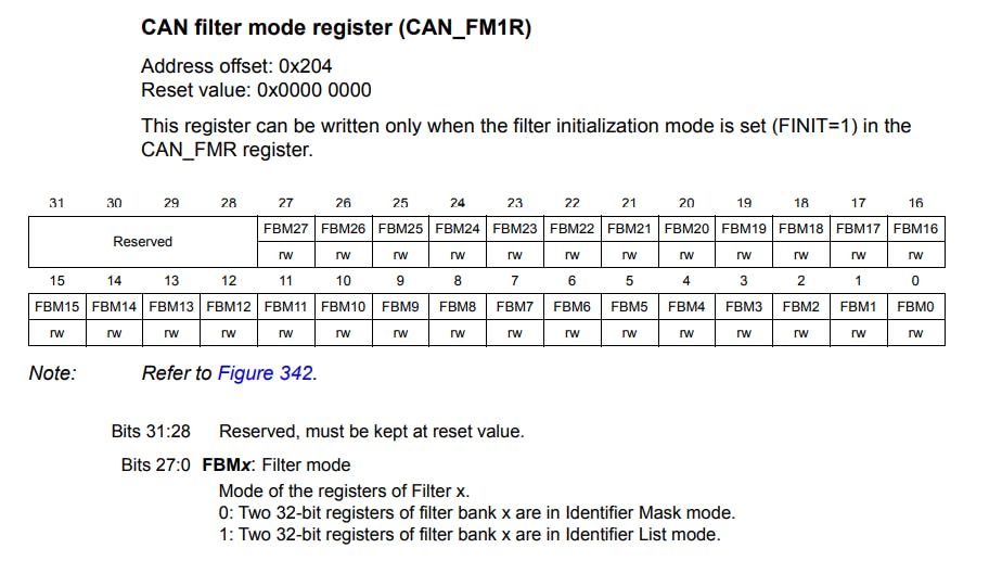
// Select Identifier List mode
CAN1->FM1R |= CAN_FM1R_FBM13;
//Activating filter 14
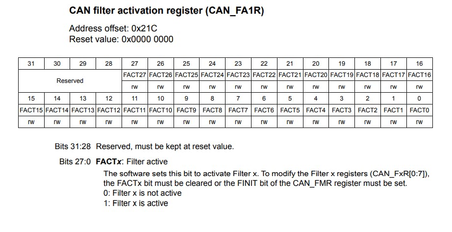
CAN1->FA1R |= CAN_FA1R_FACT13;
//Exit filter Initialization Mode
CAN1->FMR &= ~CAN_FMR_FINIT;
}
Firstly, we enable the clock for CAN1 by writing a 1 to the CAN1EN bit in the RCC->APB1ENR register. Then, we enter the Initialization Mode for CAN1 by writing a 1 to the INRQ bit in the CAN1->MCR register, and wait for the acknowledgment for entering initialization mode by polling the INAK bit in the CAN1->MSR register.
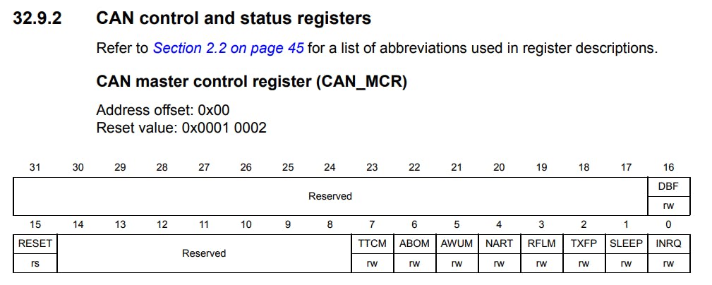
Then, we need to set the Loopback Mode as our operating mode. This is done by writing a 1 to the LBKM bit in the CAN1->BTR register. Then we need to configure the baud rate CAN. For that, I have chosen the baud rate to be 125 Kbps. CAN supports speeds up to 1 Mbps. To set up the baud rate we first set the Re-synchronization jump width to be 1. This is done by clearing the SJW[1:0] bits in the CAN1->BTR register. Since we need to set the value that is one less than the desired value. After that, we set the number of Time Quanta for Time Segment 2 which is 4. This is done by first clearing the TS2[2:0] bits and then writing 011 to them in the CAN1->BTR register. After that, we set the Time Segment 1 to have 3 Time Quanta by first clearing the TS1[3:0] bits and then writing 010 to them in the CAN1->BTR register. After this is done, we need to set our Prescaler to 16. This is done by writing 15 to the BRP[9:0] bits in the CAN1->BTR register.
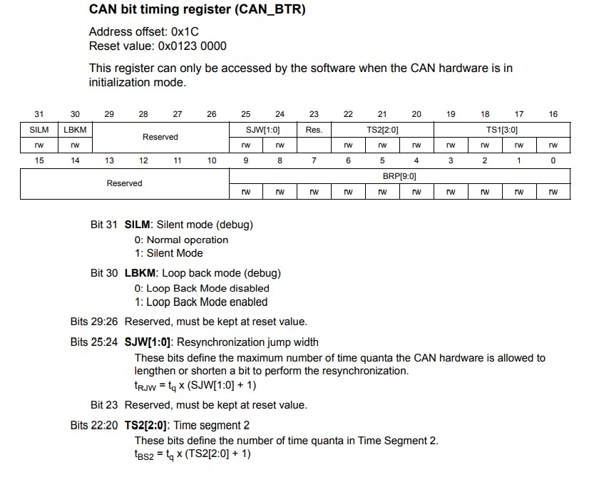
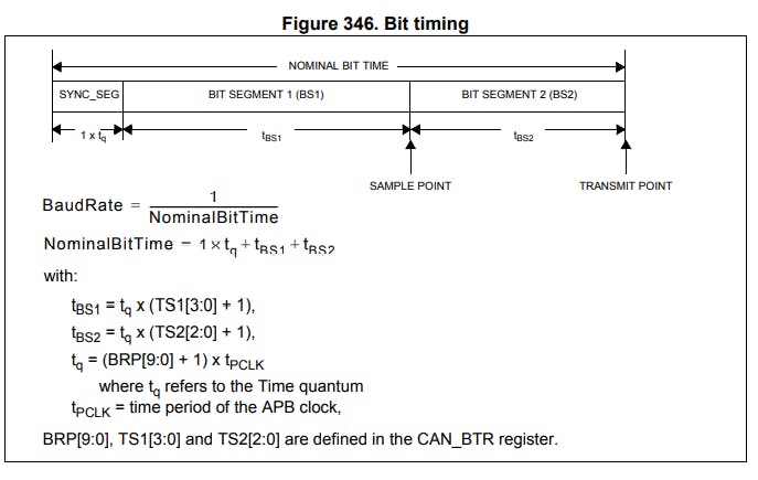
From the formulas given in the above figure, we will see how our settings result in a baud rate of 125 Kbps. Or APB1 clock is running at 16MHz so,
$$ t_{PCLK} = 1 / 16 MHz = 62.5 ns = tp $$
So,
$$ t_{q} = (BRP[9:0]+1)*(t_p) $$
$$ t_{q}= (15+1)*(62.5 ns) = 1000 ns = tq $$
And,
$$ t_{BS1} = tq*(TS1[3:0]+1) $$
$$ t_{BS1} = 1000*3 = 3000 ns $$
$$ t_{BS2} = tq*(TS2[2:0]+1) $$
$$ t_{BS2} = 1000*4 = 4000 ns $$
Therefore,
$$ Nominal Bit Time = tq + tBS1 + tBS2 $$
$$ Nominal Bit Time = 1000 + 3000 + 4000 = 8000 ns $$
Hence,
$$ Baud Rate = 1 / Nominal Bit Time = 1 / 8000 ns = 125000 bits/s $$
Then, we first exit the Initialization mode which is similar to the way we entered initialization mode, the only difference being here, we clear the INRQ bit in the CAN1->MCR register. Like this, we also exit sleep mode to wake up CAN. This is done by clearing the SLEEP bit in the CAN1->MCR register.
Now, we need to set up the Transmission Mailbox registers. Here, we chose the mailbox zero, and set its TIR register to 0. This is done by the line CAN1->sTxMailBox[0].TIR = 0. Then we configure our identifier, I have chosen the identifier to be 0x245. So, we write this value to the STID[10:0] bits in the CAN1->sTxMailbox[0].TIR register. Then we set the CAN1->sTxMailBox[0].TDHR to 0. We also need to set the number of bytes that need to be transmitted. In our case, we need to transmit one byte, so we write 1 to the CAN1->sTxMailBox[0].TDTR register.
The last step in the CAN initialization process is to configure the filters. For this, we need to enter the Filter initialization. This is done by writing a 1 to the FINIT bit in the CAN1->FMR register. There are a total of 28 filter banks available for CAN. These are split between CAN1 and CAN2. So, we need to set up this split and also specify the bank number from which the filter banks for CAN2 start. Here, I have assigned 14 filter banks to CAN1 and the remaining 14 to CAN2. Since we are not using CAN2 here, the filter banks associated with it will not matter. The Start Bank for CAN2 or the End bank for CAN1 is defined by writing 14 to the CAN2SB[5:0] bits in the CAN1->FMR register. After that, out of the 14 available banks I have used filter number 13 here. Then, we select the 32-bit Scale Configuration for the filters. This is done by writing a 1 to the FSC13 bit (signifying the 13th filter bank) in the CAN1->FS1R register. To set up the filter for discarding and keeping the messages we write a value of 0x245<<21 in the CAN1->sFilterRegister[13].FR1. This is the same as our transmission Identifier. Since we want all our Identifier bits to match while message reception is done, we choose the Identifier List Mode. This is set by writing a 1 to the FBM13 bit in the CAN1->FM1R register.
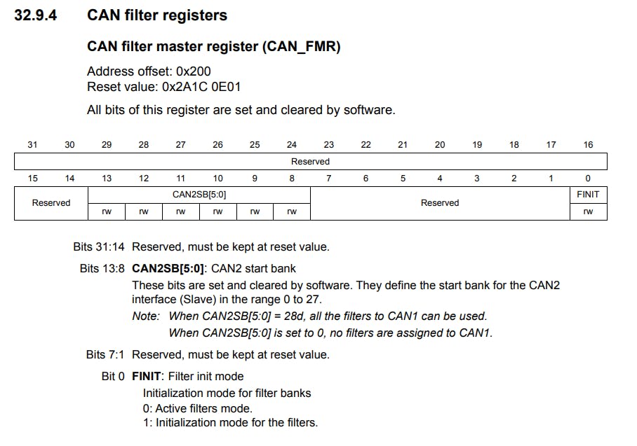
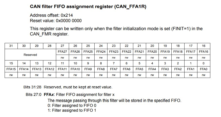
Then, the filter 13 needs to be activated by writing a 1 to the FACT13 bit in the CAN1->FA1R register. After that, we exit the Filter initialization by clearing the FINIT bit in the CAN1->FMR register. Since we did not assign any value to the FFA13 bit in the CAN1->FFA1R register it remains at its default value, that is 0, and hence, the received message gets stored in FIFO 0.
- Message Transmission is handled by the
void CAN1_Tx(uint8_t tr)function,
void CAN1_Tx(uint8_t tr){
    // Put the Data to be transmitted into Mailbox Data Low Register
    CAN1->sTxMailBox[0].TDLR = tr;

    // Request for Transmission
    CAN1->sTxMailBox[0].TIR |= 1;
}
For this, we put the data provided by the user into the CAN1->sTxMailBox[0].TDLR register. Then, a transmission request is raised by writing a 1 to the TXRQ bit in the CAN1->sTxMailBox[0].TIR register.
- For message reception, the
uint8_t CAN1_Rx()function is used,
uint8_t CAN1_Rx(){
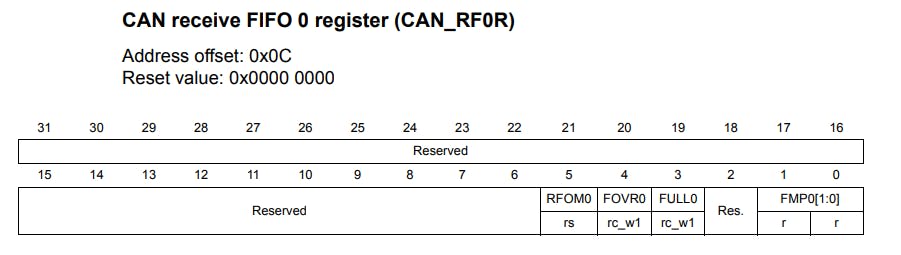
// Monitoring FIFO 0 message pending bits FMP0[1:0]
while(!(CAN1->RF0R & 3)){}
// Read the data from the FIFO 0 mailbox from Mailbox data low register
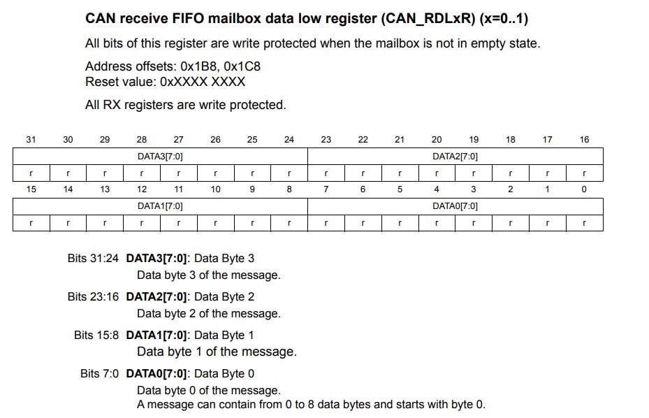
uint8_t RxD = (CAN1->sFIFOMailBox[0].RDLR) & 0xFF;
rec = RxD;
// Releasing FIFO 0 output mailbox
CAN1->RF0R |= 1<<5;
return RxD;
}
Here, we first check if there is a message pending in FIFO 0 by polling the FMP0[1:0] bits in the CAN1->RF0R register. After this, we declare a local variable uint8_t RxD that reads the received value from the CAN1->sFIFOMailBox[0].RDLR register. A Bitwise AND operation of the received value and 0xFF is performed to get the final value. Then, we release the FIFO 0 mailbox by writing a 1 to the RF0M0 bit in the CAN1->RF0R register, and we return the received value.
- The delay is provided by the
void TIM4_ms_Delay(uint32_t delay)function,
void TIM4_ms_Delay(uint32_t delay){
RCC->APB1ENR |= 1<<2; //Start the clock for the timer peripheral
TIM4->PSC = 16000-1; //Setting the clock frequency to 1kHz.
TIM4->ARR = (delay); // Total period of the timer
TIM4->CNT = 0;
TIM4->CR1 |= 1; //Start the Timer
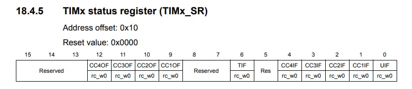
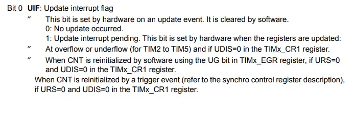
while(!(TIM4->SR & TIM_SR_UIF)){} //Polling the update interrupt flag
TIM4->SR &= ~(0x0001); //Reset the update interrupt flag
}
Here, we enable the clock for the Timer 4, and set the Pre-scalar to 16000-1 to reduce the clock speed to 1 KHz, which means one clock tick corresponds to 1ms. After that, we assign the desired delay value to the TIM2->ARR register, initialize the count to zero and start the timer. Then we poll the UIF or the Update Interrupt Flag, which is set after the desired amount of clock ticks provided in the TIM2->ARR register are done, or in other words when the timer overflows. After the UIF flag is set we clear it from the TIM2->SR register and exit the function.
4. Writing the main Function
int main(void){
    GPIO_Init();
    CAN1_Init();
    while(1){
        CAN1_Tx(k);
        rec= CAN1_Rx();
        k += 1;
        if (k>25)
            k = 0;
        TIM4_ms_Delay(1000);
    }
}
In the main function, we first configure our GPIO pins by calling the GPIO_Init() function. Then we initialize the CAN1 peripheral by calling the CAN1_Init() function. After that in a while loop, we continuously transmit a range of numbers from 1 to 25. The variable k that we declared earlier is passed as a parameter to the CAN1_Tx(k) function, and the variable rec is used to store the received value when CAN1_Rx() is called. In each iteration, we increment k by 1 and if it becomes larger than 25, we set it back to 0. After that, a delay of 1 second or 1000ms is provided using the TIM4_ms_Delay(1000) function.
This process repeats indefinitely. This completes the Loopback test on the CAN peripheral.
Conclusion
This article provided an overview of the process that is to be used to perform the Loopback test on the CAN peripheral on the STM32F407 Discovery Kit.
I hope you found this article useful and easy to follow along😀. All the codes used here are present in my GitHub repository, which you can access by clicking here.

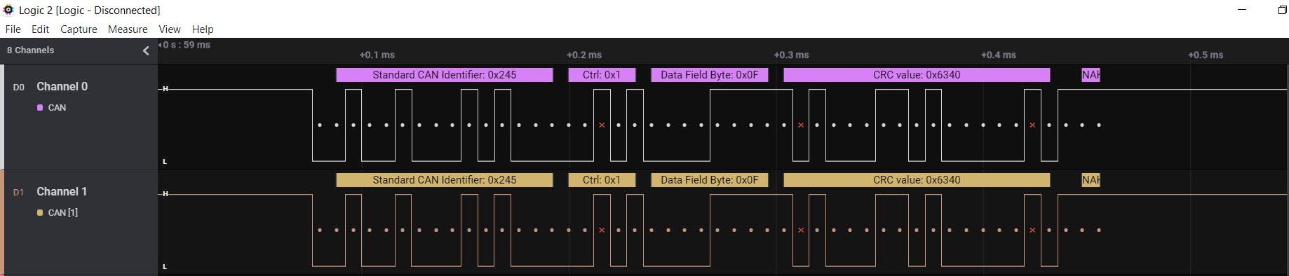
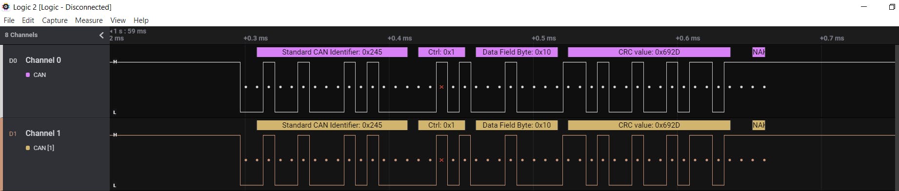
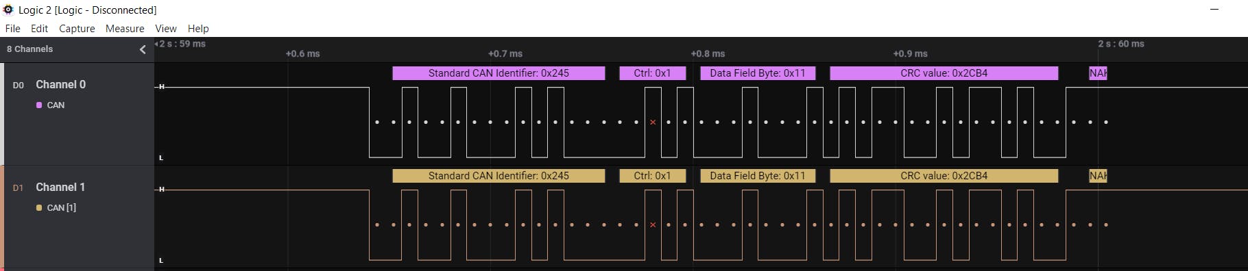
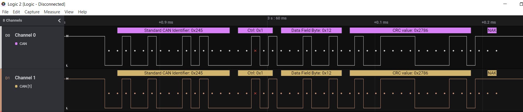
The following pictures show the various parts of the CAN Frame captured through a Logic Analyzer. The Channel 0 is connected to CAN Tx and Channel 1 is connected to CAN Rx.