Establishing Communication Between an Arduino UNO and the STM32F407 Discovery Kit using the CAN Protocol


Introduction
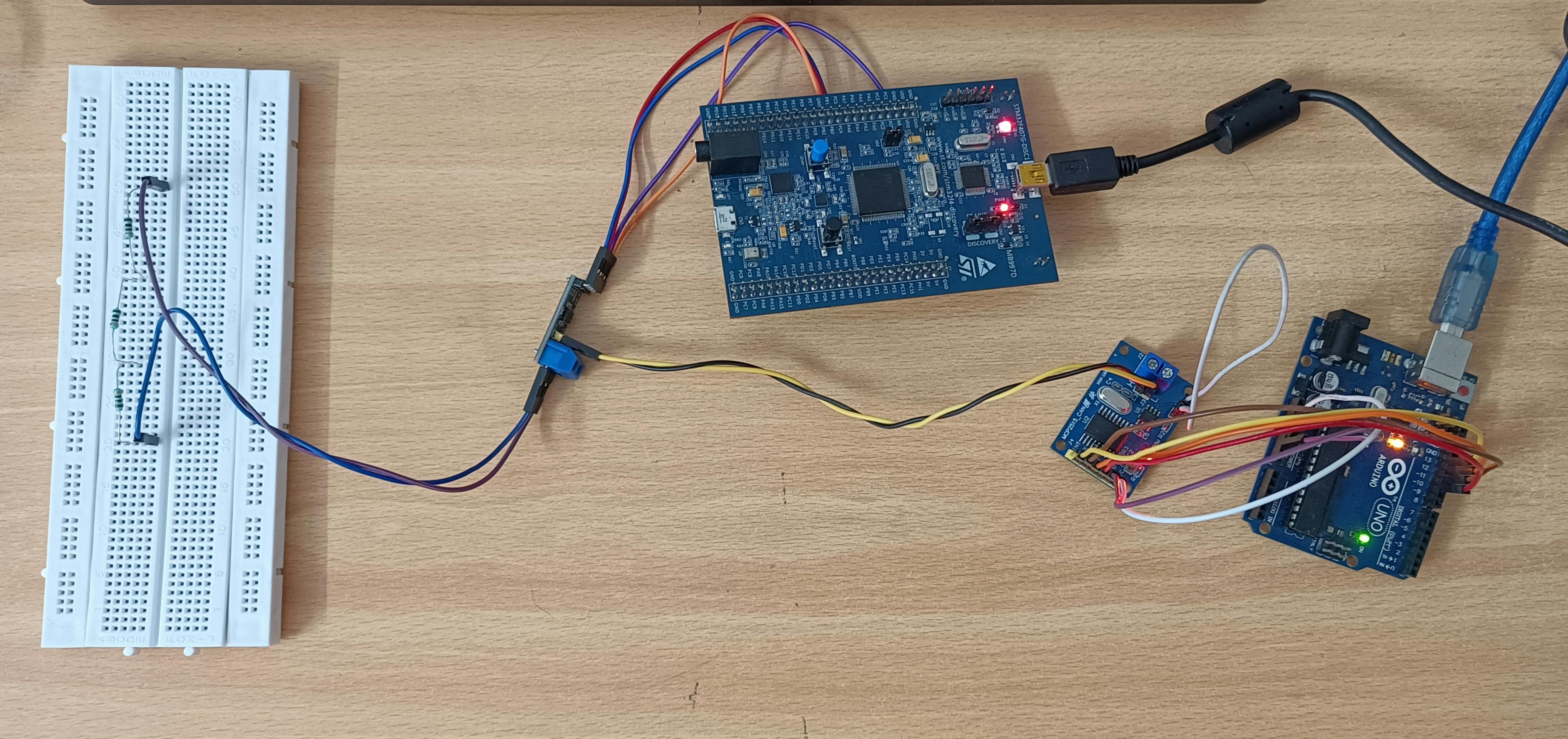
HI!! 😄 In this article we will continue our discussion on the CAN (Controller Area Network) Protocol. In this blog, I will be demonstrating the working of the CAN peripheral on the STM32F407 Discovery Kit in the Normal Mode. For the purposes of this project, I have used an Arduino UNO as the second node on the CAN Bus. We will be trying to get these two boards to transmit and receive information from one another. Here, I have set the STM32F407 Discovery Kit to be the transmitting node and the Arduino UNO to receive the messages sent by the former. Although each node can transmit and receive at the same time, both the nodes have been restricted to a single function for simplicity. The simultaneous reception and transmission on a node can be implemented in a very similar way, as is described in the further sections.
Working Principle
- CAN Protocol
In my last blog, I focused on the Loopback Mode using the CAN peripheral, in which I have explained the basics of the CAN protocol, various message frames, the elements of the message frames, and the filter configurations. So, I would recommend you to go through it, before continuing with this article, if the concept of CAN is new to you. You can read it by clicking here.
Now, let's understand how the CAN Bus moderates the various messages sent by the different nodes. This process is known as Arbitration. It happens based on the Identifier Field present in the CAN Message. By doing this, all the nodes agree on which message needs to be transmitted first, or which node will be utilizing the bus. During this, all the other nodes must remain silent or idle, except the node that has won the arbitration. Here, smaller the message identifier, higher the message priority. A dominant bit (logic 0) overrides a recessive bit (logic 1), that is if the bus is in a dominant state (i.e at logic 0), a single node cannot pull the bus to a recessive state. This can only be done if all the nodes pull the bus up to the recessive state simultaneously. Hence, the name dominant bit.
A CAN node monitors the bus while transmitting a message, if it detects a dominant bit when it has transmitted a recessive bit, it will immediately stop transmission and become a receiver. The node that wins the transmission at the end is the one that transmits and detects the same bit while monitoring the bus. This node continues to transmit its message, while the other nodes have to wait for the bus to get idle again for re-transmitting. This is how transmission conflicts are resolved during CAN transmission. This helps maintain error-free and efficient communication between the nodes.
- MCP2515 and TJA1050: CAN Controller and Transceiver
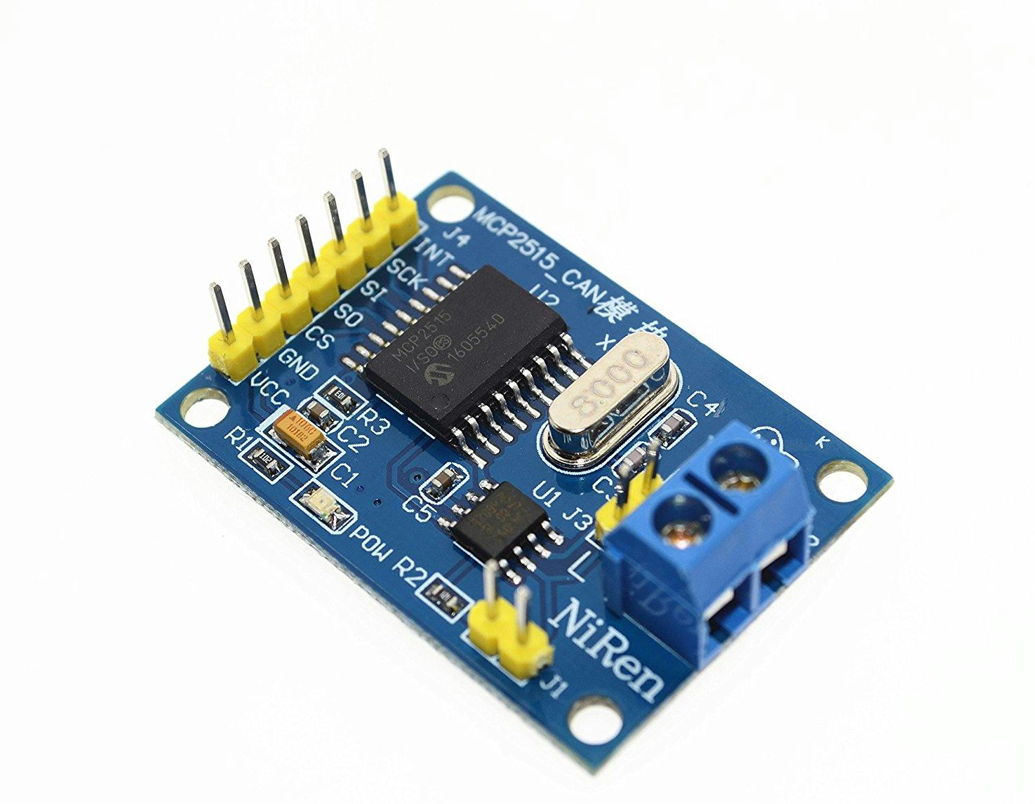
The ATMega 328 microcontroller present on the Arduino UNO does not have a CAN controller present on board. So, we need to connect the CAN controller as well as the CAN Transceiver externally. We interface the MCP2515 (CAN Controller) with the ATMega 328 using the SPI Protocol. I will be discussing the SPI Protocol in detail, in a later blog. For the purposes of this project, SPI is just another synchronous serial communication protocol that can be configured to work as a 4-wire or a 3-wire protocol. It is a Single Master Multi Slave full-duplex type of protocol. The various lines used are, MISO (Master In Slave Out), MOSI (Master Out Slave In), SCK (Serial Data Clock), and CS (Chip Select). Each slave is accessed by the CS line.
In this project, I have used a breakout board containing both the MCP2515 and TJA1050. Also, this CAN module has an onboard 120-ohm bus termination, which can be enabled by shorting the J1 terminals using a jumper wire.
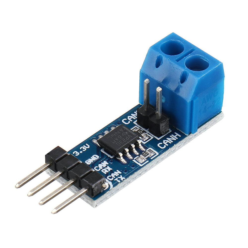
Since the STM32F407 Discovery Kit already has a CAN controller, we just need to connect a transceiver externally. Here, I have used the SN65HVD230 CAN Transceiver.
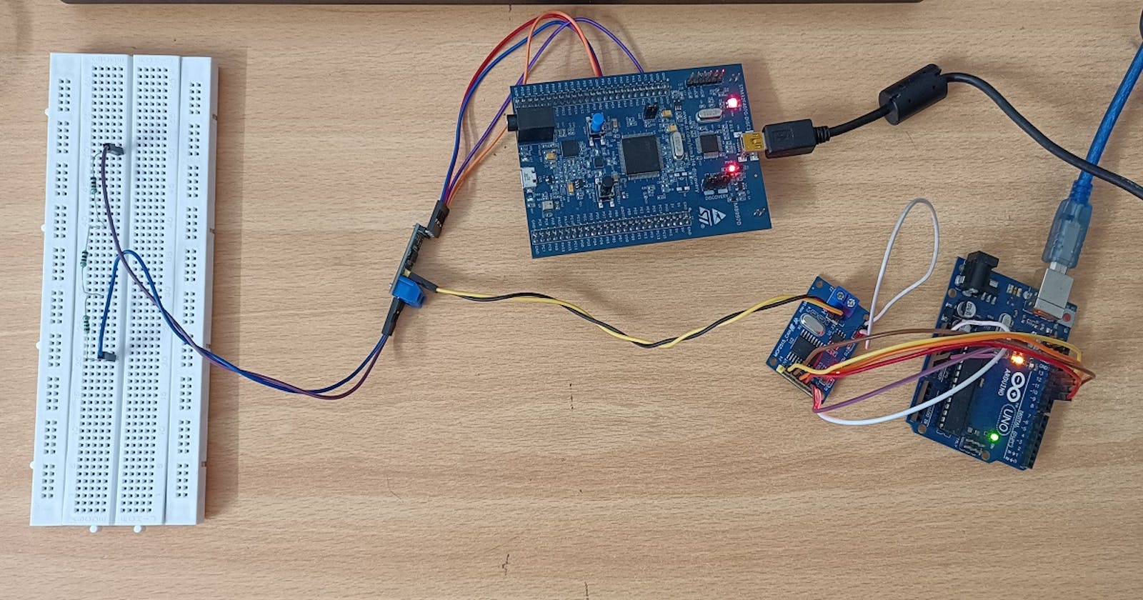
The connections that need to be made are given in my GitHub repository, which can be accessed by clicking here.
Components Required
An STM32F4 based MCU
An Arduino UNO
CAN Module containing CAN Transceiver and CAN Controller
A SN65HVD230 Breakout board
A 120-ohm resistor OR any combination of registers that results in 120-ohms ( I have used two 10-ohm resistors and a 100-ohm resistor and connected them in series to get 120-ohms).
A Logic Analyzer
A Few Jumper Wires
A breadboard
These are the components required to get started with this project. Let's dive into the code now.
Programming the STM32F407
The code used here is very similar to the one I have used in my last blog on the Loopback Test on the CAN Peripheral. There are very few changes, but I will be explaining the code here also. Although we are only transmitting from this node, I have written the function for receiving data and the filters also have been configured. Here, I am trying to transmit the numbers from 1-25 from the STM32F407 to the Arduino UNO.
1. Including the necessary Header Files and some comments about the code
/******************************************************************************
 * Configurations are made as follows:
 * PB8 - CAN1_RX (Need to be set in AF9 for CAN1/CAN2)
 * PB9 - CAN1_TX (Need to be set in AF9 for CAN1/CAN2)
 *
 * The following is a bare-metal code written for CAN Normal Communication test
 * on the Arm Cortex-M4 based STM32F407 Discovery Kit.
 *
 * @File   main.c
 *****************************************************************************/

#include "stm32f4xx.h"
#define ARM_MATH_CM4
These are the header files included at the top of our main.c file. The stm32f4xx.h is the one for our microcontroller and the ARM_MATH_CM4 is for any math operations that we perform in our code.
2. Declaring the User-Defined Functions and variables
void GPIO_Init(void);
void CAN1_Init(void);
void CAN1_Tx(uint8_t tr);
uint8_t CAN1_Rx(void);
void TIM4_ms_Delay(uint32_t delay);
uint8_t k = 0;
uint8_t rec = 0;
The void GPIO_Init(void) function is used to initialize and configure the GPIO pins that we will be needing to connect our SN65HVD230 module and use the CAN Peripheral. The void CAN1_Init(void) and the void CAN1_Tx(uint8_t tr) functions are used to initialize CAN1 and transmit a byte of data respectively. The uint8_t CAN1_Rx(void) function is used to receive incoming data. void TIM4_ms_Delay(uint32_t delay) acts as our delay function which utilizes the TIM4 peripheral and provides a delay in milliseconds. Finally, we declare the variables uint8_t k and uint8_t rec which will use to transmit and receive data respectively.
3. Defining the User-Defined Functions
- Let's configure the GPIO pins using the
void GPIO_Init()function,
void GPIO_Init(){
// Enable GPIOA clock signal
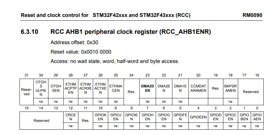
RCC->AHB1ENR |= RCC_AHB1ENR_GPIOBEN;
// Configuring PB8 and PB9 in alternate function mode
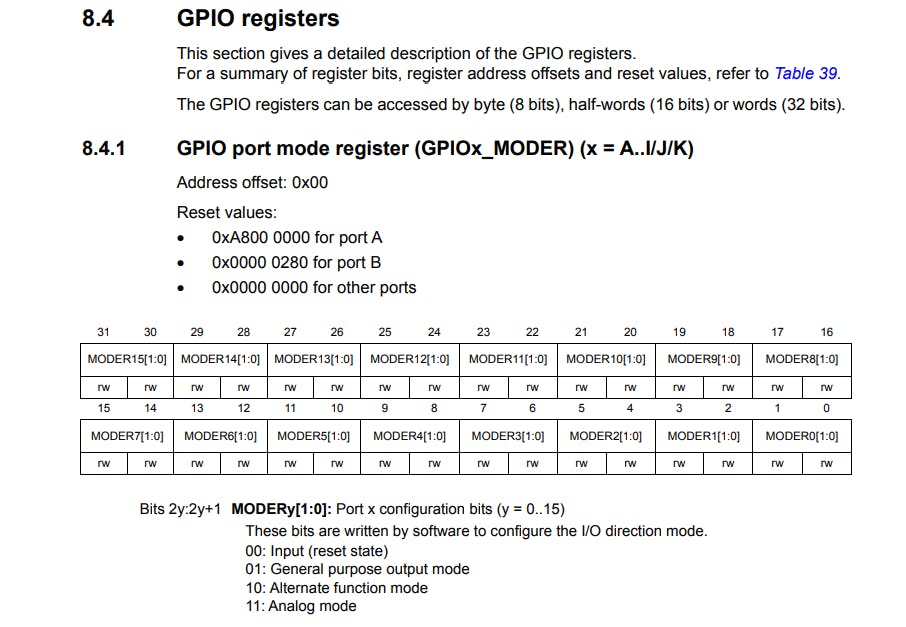
GPIOB->MODER |= (GPIO_MODER_MODER8_1 | GPIO_MODER_MODER9_1);
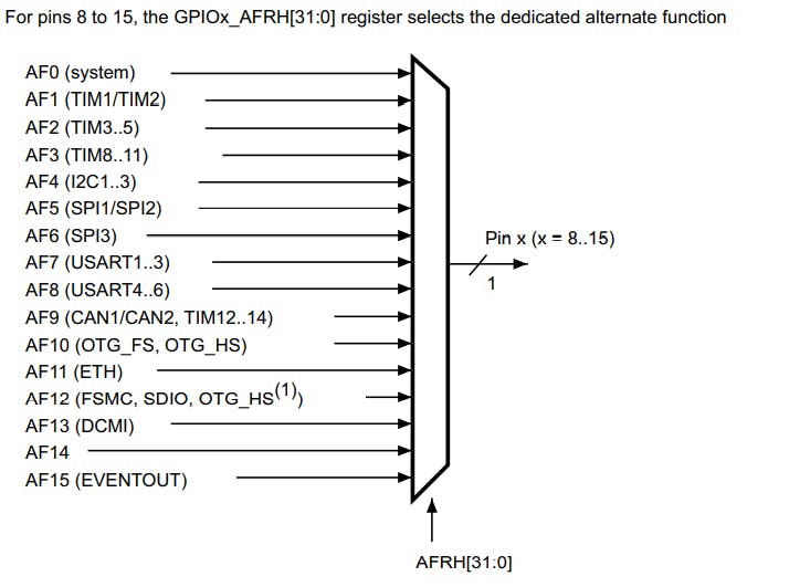
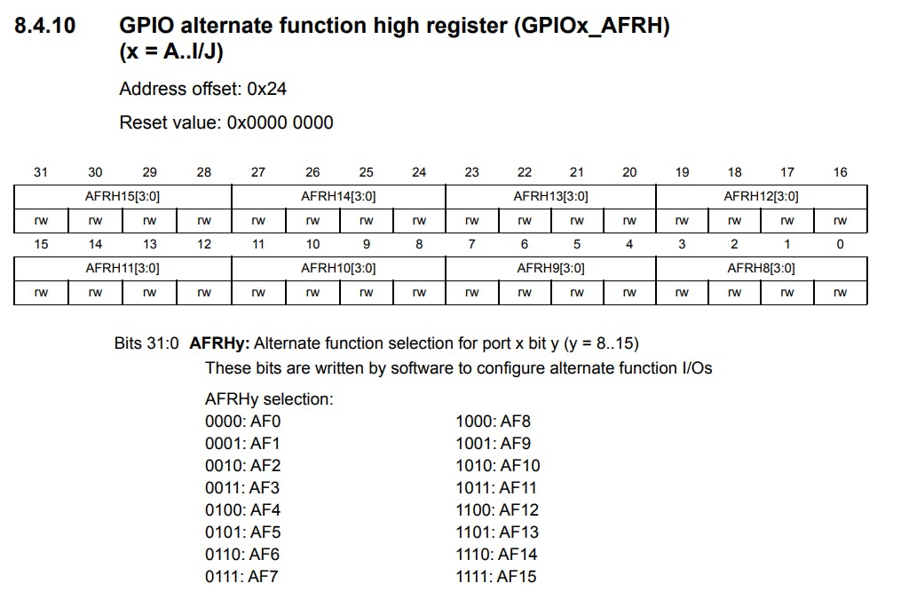
// Selecting AF9 for PB8 and PB9 (See Page 272 of dm00031020)
GPIOB->AFR[1] |= (GPIO_AFRH_AFSEL8_3 | GPIO_AFRH_AFSEL8_0 |
GPIO_AFRH_AFSEL9_0 | GPIO_AFRH_AFSEL9_3);
}
First, we enable the GPIOA clock by writing a 1 to the GPIOBEN bit in the RCC->AHB1ENR register.
Then, we set PB8 and PB9 in Alternate-Function Mode. This is done by writing 10 to the MODER8[1:0] and MODER9[1:0] bits in the GPIOB->MODER register.
We need to select AF9 for the CAN1 peripheral. This is done by writing 1001 to the AFRH8[3:0] and the AFRH9[3:0] bits in the GPIOB->AFR[1] register.
- Then, we come to our
void CAN1_Init()where we initialize and configure theCAN1peripheral,
void CAN1_Init(){
/* 1. Setting Up the Baud Rate and Configuring CAN1 in
* Normal Mode -------------------------------------------------------*/
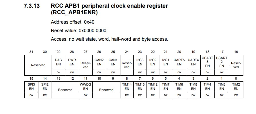
// Enable clock for CAN1
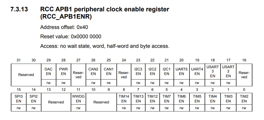
RCC->APB1ENR |= RCC_APB1ENR_CAN1EN;
// Entering CAN Initialization Mode and wait for acknowledgment
CAN1->MCR |= CAN_MCR_INRQ;
while (!(CAN1->MSR & CAN_MSR_INAK)){}
//Exit Sleep Mode
CAN1->MCR &= ~CAN_MCR_SLEEP;
while (CAN1->MSR & CAN_MSR_SLAK){}
//Set Loop back mode for CAN1
//CAN1->BTR |= CAN_BTR_LBKM;
//Setting the Re synchronization jump width to 1
CAN1->BTR &= ~CAN_BTR_SJW;
//Setting the no. of time quanta for Time segment 2
// TS2 = 4-1;
CAN1->BTR &= ~(CAN_BTR_TS2);
CAN1->BTR |= (CAN_BTR_TS2_1 | CAN_BTR_TS2_0);
//Setting the no. of time quanta for Time segment 1
// TS1 = 3-1;
CAN1->BTR &= ~(CAN_BTR_TS1);
CAN1->BTR |= (CAN_BTR_TS1_1);
//Setting the Baud rate Pre-scalar for CAN1
// BRP[9:0] = 16-1
CAN1->BTR |= ((16-1)<<0);
/* 2. Configuring the Filters--------------------------------------------*/
//Enter Filter Initialization mode to configure the filters
CAN1->FMR |= CAN_FMR_FINIT;
// Configuring the Number of Filters Reserved for CAN1
// and also the start bank for CAN2
CAN1->FMR |= 14<<8;
// Select the single 32-bit scale configuration
CAN1->FS1R |= CAN_FS1R_FSC13;
// Set the receive ID
CAN1->sFilterRegister[13].FR1 = 0x103<<21;
// Select Identifier List mode
CAN1->FM1R |= CAN_FM1R_FBM13;
//Activating filter 13
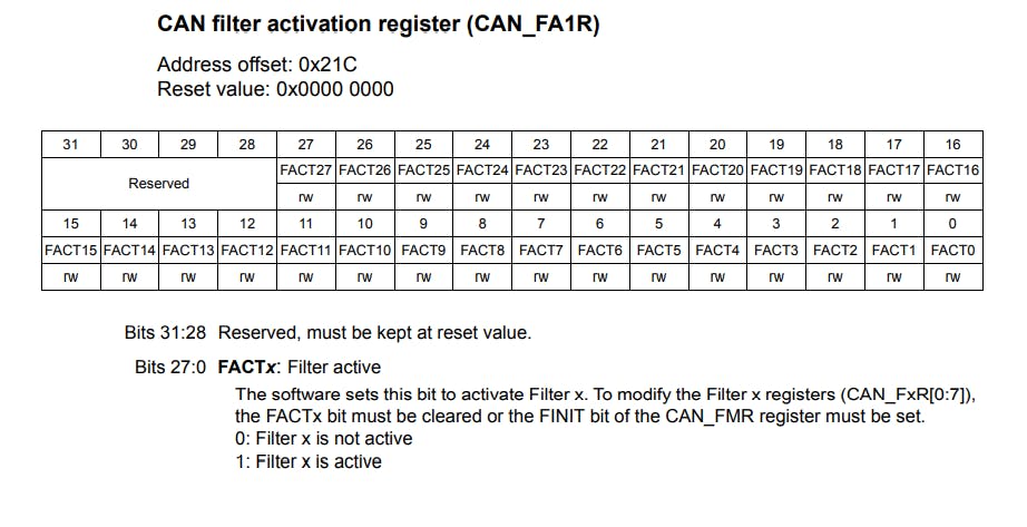
CAN1->FA1R |= CAN_FA1R_FACT13;
//Exit filter Initialization Mode
CAN1->FMR &= ~CAN_FMR_FINIT;
/* 3. Setting up the Transmission----------------------------------------*/
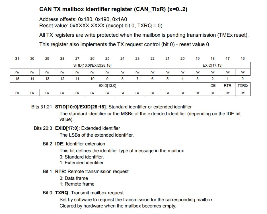
CAN1->sTxMailBox[0].TIR = 0;
//Setting up the Std. ID
CAN1->sTxMailBox[0].TIR = (0x245<<21);
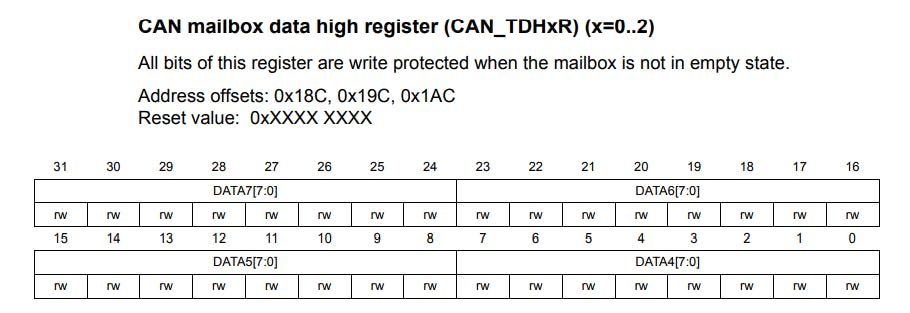
CAN1->sTxMailBox[0].TDHR = 0;
// Setting Data Length to 1 Byte.
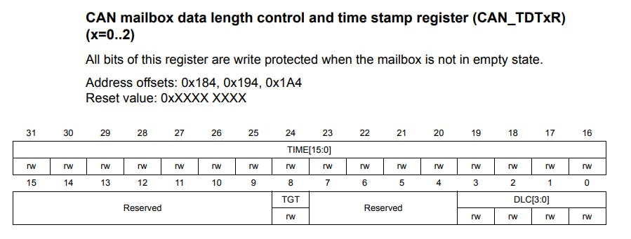
CAN1->sTxMailBox[0].TDTR = 1;
// Exit the Initialization mode for CAN1
// Wait until the INAK bit is cleared by hardware
CAN1->MCR &= ~CAN_MCR_INRQ;
while (CAN1->MSR & CAN_MSR_INAK){}
}
Firstly, we enable the clock for CAN1 by writing a 1 to the CAN1EN bit in the RCC->APB1ENR register. Then, we enter the Initialization Mode for CAN1 by writing a 1 to the INRQ bit in the CAN1->MCR register, and wait for the acknowledgment for entering initialization mode by polling the INAK bit in the CAN1->MSR register.
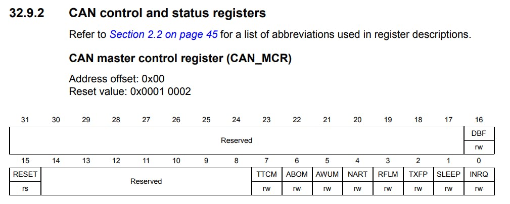
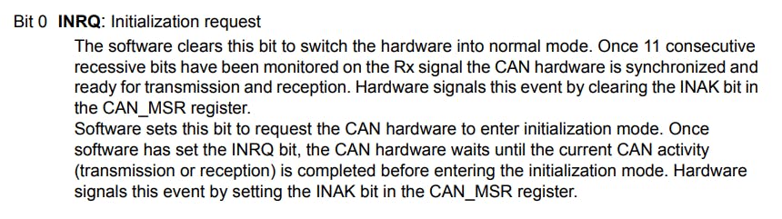
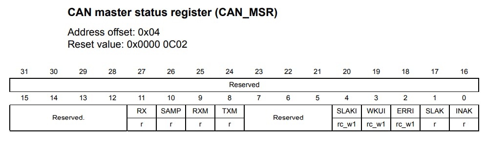
Then, we need to set our operating mode as Normal, which is automatically done after we exit the sleep mode of the CAN peripheral. We exit sleep mode to wake up CAN. This is done by clearing the SLEEP bit in the CAN1->MCR register.CAN Loopback Mode can be set by the following step. This is done by writing a 1 to the LBKM bit in the CAN1->BTR register. Then we need to configure the baud rate CAN. For that, I have chosen the baud rate to be 125 Kbps. CAN supports speeds up to 1 Mbps. To set up the baud rate we first set the Re-synchronization jump width to be 1. This is done by clearing the SJW[1:0] bits in the CAN1->BTR register. Since we need to set the value that is one less than the desired value. After that, we set the number of Time Quanta for Time Segment 2 which is 4. This is done by first clearing the TS2[2:0] bits and then writing 011 to them in the CAN1->BTR register. After that, we set the Time Segment 1 to have 3 Time Quanta by first clearing the TS1[3:0] bits and then writing 010 to them in the CAN1->BTR register. After this is done, we need to set our Prescaler to 16. This is done by writing 15 to the BRP[9:0] bits in the CAN1->BTR register.
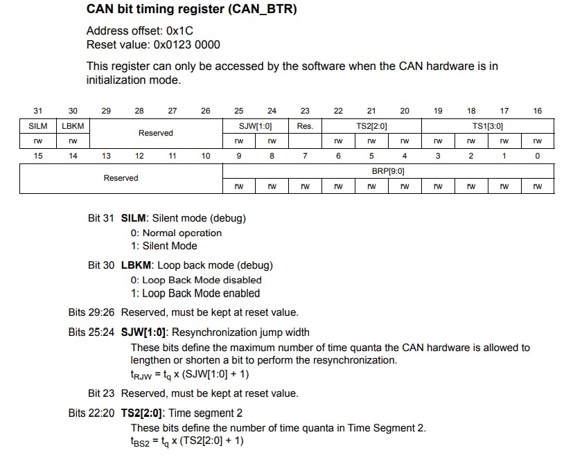
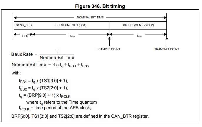
From the formulas given in the above figure, we will see how our settings result in a baud rate of 125 Kbps. Or APB1 clock is running at 16MHz so,
$$t_{PCLK} = 1 / 16 MHz = 62.5 ns = tp$$
So,
$$t_{q} = (BRP[9:0]+1)*(t_p)$$
$$t_{q}= (15+1)*(62.5 ns) = 1000 ns = tq$$
And,
$$t_{BS1} = tq*(TS1[3:0]+1)$$
$$t_{BS1} = 1000*3 = 3000 ns$$
$$t_{BS2} = tq*(TS2[2:0]+1)$$
$$t_{BS2} = 1000*4 = 4000 ns$$
Therefore,
$$Nominal Bit Time = tq + tBS1 + tBS2$$
$$Nominal Bit Time = 1000 + 3000 + 4000 = 8000 ns$$
Hence,
$$Baud Rate = 1 / Nominal Bit Time = 1 / 8000 ns = 125000 bits/s$$
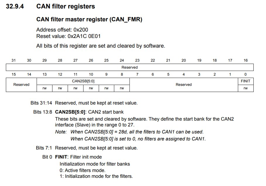
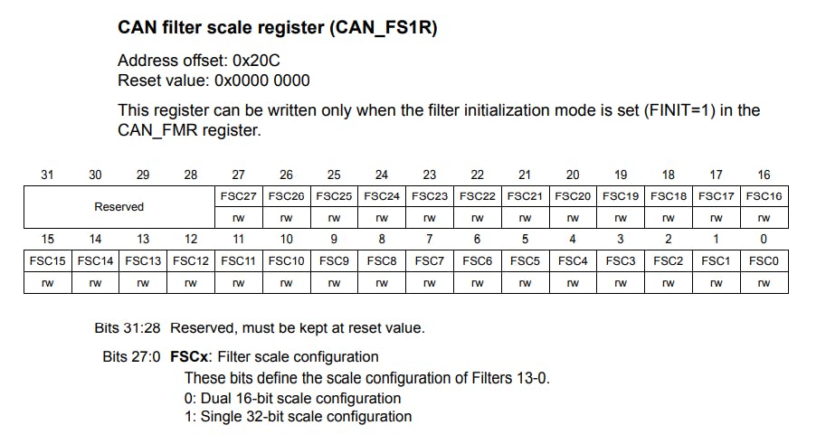
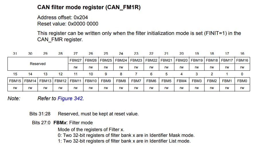
The next step in the CAN initialization process is to configure the filters. For this, we need to enter the Filter initialization. This is done by writing a 1 to the FINIT bit in the CAN1->FMR register. There are a total of 28 filter banks available for CAN. These are split between CAN1 and CAN2. So, we need to set up this split and also specify the bank number from which the filter banks for CAN2 start. Here, I have assigned 14 filter banks to CAN1 and the remaining 14 to CAN2. Since we are not using CAN2 here, the filter banks associated with it will not matter. The Start Bank for CAN2 or the End bank for CAN1 is defined by writing 14 to the CAN2SB[5:0] bits in the CAN1->FMR register. After that, out of the 14 available banks I have used filter number 13 here. Then, we select the 32-bit Scale Configuration for the filters. This is done by writing a 1 to the FSC13 bit (signifying the 13th filter bank) in the CAN1->FS1R register. To set up the filter for discarding and keeping the messages we write a value of 0x103<<21 in the CAN1->sFilterRegister[13].FR1. This can be the identifier for the Arduino UNO if in case it is configured to transmit something. Here, we are not doing that, this is just to show how that configuration can be achieved. Since we want all our Identifier bits to match while message reception is done, we choose the Identifier List Mode. This is set by writing a 1 to the FBM13 bit in the CAN1->FM1R register.
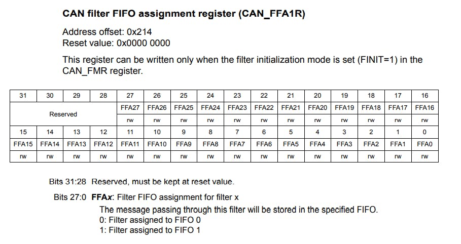
Then, the filter 13 needs to be activated by writing a 1 to the FACT13 bit in the CAN1->FA1R register. After that, we exit the Filter initialization by clearing the FINIT bit in the CAN1->FMR register. Since we did not assign any value to the FFA13 bit in the CAN1->FFA1R register it remains at its default value, that is 0, and hence, the received message gets stored in FIFO 0.
Now, we need to set up the Transmission Mailbox registers. Here, we chose the mailbox zero, and set its TIR register to 0. This is done by the line CAN1->sTxMailBox[0].TIR = 0. Then we configure our identifier, I have chosen the identifier to be 0x245. So, we write this value to the STID[10:0] bits in the CAN1->sTxMailbox[0].TIR register. Then we set the CAN1->sTxMailBox[0].TDHR to 0. We also need to set the number of bytes that need to be transmitted. In our case, we need to transmit one byte, so we write 1 to the CAN1->sTxMailBox[0].TDTR register.
Then, we need to exit the Initialization mode which is similar to the way we entered initialization mode, the only difference being here, we clear the INRQ bit in the CAN1->MCR register.
- Message Transmission is handled by the
void CAN1_Tx(uint8_t tr)function,
void CAN1_Tx(uint8_t tr){
    // Put the Data to be transmitted into Mailbox Data Low Register
    CAN1->sTxMailBox[0].TDLR = tr;

    // Request for Transmission
    CAN1->sTxMailBox[0].TIR |= 1;
}
For this, we put the data provided by the user into the CAN1->sTxMailBox[0].TDLR register. Then, a transmission request is raised by writing a 1 to the TXRQ bit in the CAN1->sTxMailBox[0].TIR register.
- For message reception, the
uint8_t CAN1_Rx()function is used. I have written this function to showcase how simultaneous message reception and transmission can be done.
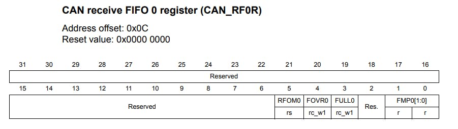
uint8_t CAN1_Rx(){
// Monitoring FIFO 0 message pending bits FMP0[1:0]
while(!(CAN1->RF0R & 3)){}
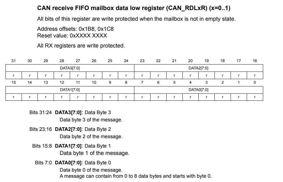
// Read the data from the FIFO 0 mailbox from Mailbox data low register
uint8_t RxD = (CAN1->sFIFOMailBox[0].RDLR) & 0xFF;
rec = RxD;
// Releasing FIFO 0 output mailbox
CAN1->RF0R |= 1<<5;
return RxD;
}
Here, we first check if there is a message pending in FIFO 0 by polling the FMP0[1:0] bits in the CAN1->RF0R register. After this, we declare a local variable uint8_t RxD that reads the received value from the CAN1->sFIFOMailBox[0].RDLR register. A Bitwise AND operation of the received value and 0xFF is performed to get the final value. Then, we release the FIFO 0 mailbox by writing a 1 to the RF0M0 bit in the CAN1->RF0R register, and we return the received value.
- The delay is provided by the
void TIM4_ms_Delay(uint32_t delay)function,
void TIM4_ms_Delay(uint32_t delay){
RCC->APB1ENR |= 1<<2; //Start the clock for the timer peripheral
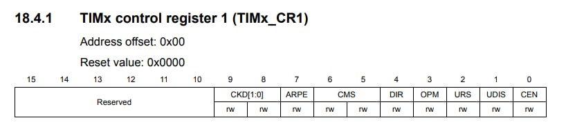
TIM4->PSC = 16000-1; //Setting the clock frequency to 1kHz.
TIM4->ARR = (delay); // Total period of the timer
TIM4->CNT = 0;
TIM4->CR1 |= 1; //Start the Timer
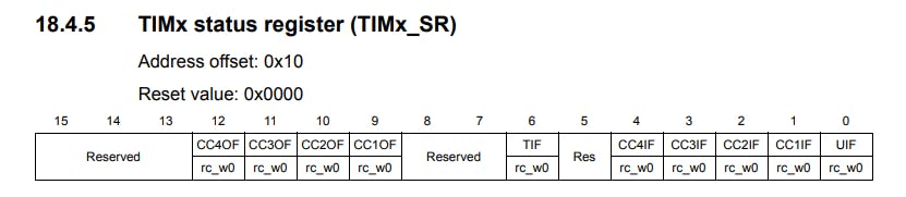
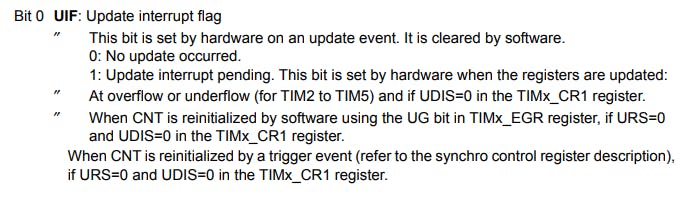
while(!(TIM4->SR & TIM_SR_UIF)){} //Polling the update interrupt flag
TIM4->SR &= ~(0x0001); //Reset the update interrupt flag
}
Here, we enable the clock for the Timer 4, and set the Pre-scalar to 16000-1 to reduce the clock speed to 1 KHz, which means one clock tick corresponds to 1ms. After that, we assign the desired delay value to the TIM2->ARR register, initialize the count to zero and start the timer. Then we poll the UIF or the Update Interrupt Flag, which is set after the desired amount of clock ticks provided in the TIM2->ARR register are done, or in other words when the timer overflows. After the UIF flag is set we clear it from the TIM2->SR register and exit the function.
4. Writing the main Function
int main(void){
    GPIO_Init();
    CAN1_Init();
    while(1){
        CAN1_Tx(k);
        //rec= CAN1_Rx();
        k += 1;
        if (k>25)
            k = 0;
        TIM4_ms_Delay(1000);
    }
}
In the main function, we first configure our GPIO pins by calling the GPIO_Init() function. Then we initialize the CAN1 peripheral by calling the CAN1_Init() function. After that in a while loop, we continuously transmit a range of numbers from 1 to 25. The variable k that we declared earlier is passed as a parameter to the CAN1_Tx(k) function, and the variable rec is used to store the received value when CAN1_Rx() is called. The reception line is commented since it is not used in this particular project. In each iteration, we increment k by 1 and if it becomes larger than 25, we set it back to 0. After that, a delay of 1 second or 1000ms is provided using the TIM4_ms_Delay(1000) function.
This process repeats indefinitely. This completes the working of the Normal Mode on the CAN peripheral, in the STM32F407.
Now let's have a look at the Arduino Uno code.
Programming the Arduino UNO
For this, I have used a CAN library provided here, for configuring the MCP2515. The code is taken majorly from the example code provided in the above repository.
/***********************************************************************
 * The connection are as follows:
 * CS   - D10
 * MOSI - D11
 * MISO - D12
 * SCK  - D13
*/

#include <SPI.h>
#include<mcp2515.h>

struct can_frame canMsg;
MCP2515 mcp2515(10);


void setup() {
  Serial.begin(115200);
  SPI.begin();
  mcp2515.reset();
  mcp2515.setBitrate(CAN_125KBPS,MCP_8MHZ);
  mcp2515.setNormalMode();
  Serial.println("------- CAN Read ----------");
  Serial.println("ID  DLC   DATA");
}

void loop() {
  if (mcp2515.readMessage(&canMsg) == MCP2515::ERROR_OK) {
    Serial.print(canMsg.can_id, HEX); // print ID
    Serial.print(" ");
    Serial.print(canMsg.can_dlc, DEC); // print DLC
    Serial.print(" ");

    for (int i = 0; i<canMsg.can_dlc; i++)  {  // print the data
      Serial.print(canMsg.data[i],DEC);
      Serial.print(" ");
    }
    Serial.println();
  }
}
Firstly, we include the necessary header files like the SPI.h and mcp2515.h. Then we initialize the CAN frame as a struct. The MCP2515 is initialized by calling the mcp2515(10) function, where the pin number connected to CS is passed as its parameter.
Then in the void setup() function, we set the baud rate to 115200, for the communication between the host and the Arduino. Then, we begin the SPI communication by calling the SPI.begin() function. After, that we reset the MCP2515 by calling the mcp2515.reset() function. Then the Baud Rate for the CAN communication and the clock speed for the CAN Controller is configured by passing CAN_125KBPS and MCP_8MHZ as parameters to the mcp2515.setBitrate(CAN_125KBPS,MCP_8MHZ) function. Finally, we set the Normal Mode for communication by calling the mcp2515.setNormalMode() function. Then, we print some information on the Serial Monitor for our reference.
In the void loop() we first check if there was an error while receiving the CAN frame by the line if (mcp2515.readMessage(&canMsg) == MCP2515::ERROR_OK). After that is done, and no error is detected we print the CAN message ID, in Hex format, and the Data Length in the Decimal format. After that, we print the received data one by one in the Decimal format using a for loop which runs up to the Data Length. Then, we go to a new line before leaving the current iteration of the infinite loop.
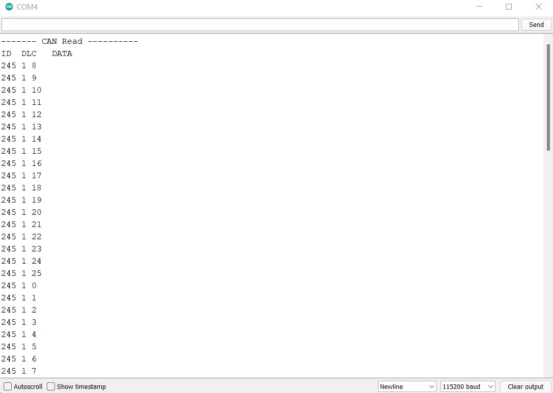
This is done infinitely, and the received data is continuously printed on the Serial Monitor on the Arduino IDE.
Conclusion
This article was aimed at providing an idea about the basic functioning of the CAN communication Protocol, and how two nodes can send and receive data using it.
I hope you found this article useful and easy to follow along😀. All the codes used here are present in my GitHub repository, which you can access by clicking here.
The received messages can be seen in the Serial Monitor in the Arduino IDE, as shown below.
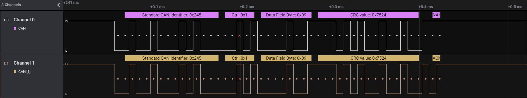
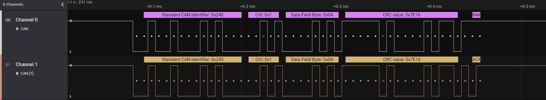
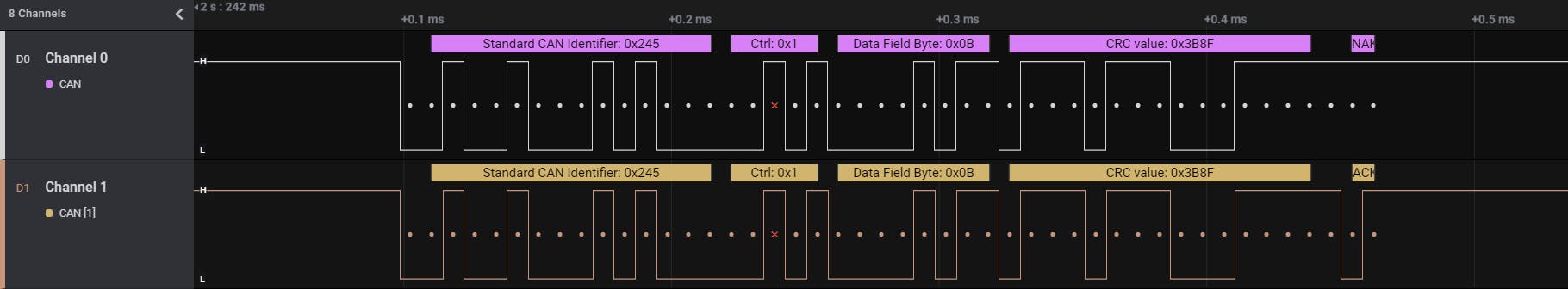
The following pictures show the various parts of the CAN Frame captured through a Logic Analyzer. Channel 0 is connected to CAN Tx and Channel 1 is connected to CAN Rx.